State Key Laboratory of Advanced Optical Communication Systems and Networks, Department of Electronic Engineering, Shanghai Jiao Tong University, Shanghai 200240, China
This Letter theoretically and experimentally studies the response of photonic switching in a channel-interleaved photonic analog-to-digital converter (PADC) with high sampling rate and wide input frequency range. A figure of merit (FoM) is introduced to evaluate the switching response of the PADC when a dual-output Mach–Zehnder modulator (MZM) serves as the photonic switch to parallelize the sampled pulse train into two channels. After the optimization of the FoM and utilization of the channel-mismatch compensation algorithm, the system bandwidth of PADC is expanded and the signal-to-distortion ratio is enhanced.
The increasing demand for the processing of signals with high frequency and wide bandwidth in modern scientific research and engineering requires signal acquisition technology with high sampling speed and high resolution[1–5]. There is a well-known electronic bottleneck of electronic analog-to-digital converters (EADCs), which is essentially limited by the timing jitter at the level of 100 fs. Besides, the analog bandwidth of EADCs is only a few gigahertz[6]. Thanks to the low timing jitter and broad bandwidth of photonics, photonic analog-to-digital converters (PADCs)[7,8] offer an alternative solution to overcome the bottleneck faced by EADCs. The feasibility of PADCs in breaking through the bandwidth limitation of EADCs has been verified in radar systems[1–4].
Among several schemes of PADCs, photonic sampling and electronic quantizing analog-to-digital converters (ADCs)[7,8] can achieve high sampling speed and high resolution. A stable mode-locked laser (MLL) with low timing jitter[9,10] serves as the sampling source, which guarantees a precise sampling time and a digitized signal with low jitter-limited noise floor. A photonic modulator with a wide input frequency range serves as a photonic sampling gate to enlarge the analog input frequency range. In order to reduce the sampling speed as well as the input frequency range at the electronic backend, high-speed PADC systems ought to be demultiplexed into multiple channels[11–15]. To take advantage of the wide bandwidth of photonics, an array of photonic switches can be laid in front of the photo-diode (PD) array[16,17] for photonic demultiplexing (i.e., channel interleaving). The electronic backend consists of an array of parallel EADCs with lower speed, narrower bandwidth, and higher precision, resulting in a wide input frequency range and a high sampling speed, which is the product of the sampling rate of a single EADC and the number of channels.
Bell et al. first demonstrated the photonic-switch-based channel-interleaved PADC system to obtain 2.8 bits effective number of bits (ENOB) with a sampling rate of 2 GS/s[17]. Later, a 505 MS/s channel-interleaved PADC system[8], which includes a one-to-eight photonic switch, was reported with the maximum ENOB of 8.2 bits, and a calibration technique[18] was developed for the suppression of channel-mismatch distortion. Up to date, the laser sources utilized were mostly passively MLLs (PMLLs)[8,16–18]. Due to the limited repetition rate of PMLLs, this scheme cannot simultaneously satisfy the requirements of high sampling speed and wide input frequency range. With the development of MLLs with higher repetition rate, we have recently investigated the pulse shape mismatch of the sampling clock in a channel-interleaved PADC[15], which provides a flat frequency response within a wide input frequency range. However, the effect of the photonic switches on the channel-interleaved PADC has not been thoroughly studied.
Sign up for Chinese Optics Letters TOC. Get the latest issue of Chinese Optics Letters delivered right to you!Sign up now
In this Letter, we investigate theoretically and experimentally the switching response of the channel-interleaved PADC. Combined with the spectral analysis[7,15], a figure of merit (FoM) that evaluates the effect of the photonic switch in the channel-interleaved PADC is defined, and a numerical simulation of the impact of the FoM on the parameters of the photonic switch is performed. In the experiment, an actively MLL (AMLL) with high repetition rate serves as the optical sampling clock, and a dual-output Mach–Zehnder modulator (MZM) is used as the photonic switch. Under the optimization of the FoM, the pulse train of the AMLL is correspondingly demultiplexed into two channels by the dual-output MZM, and the digitized data of the two channels is interleaved in the digital domain and reconstructed by the channel-mismatch compensation algorithm to suppress mismatch spurs.
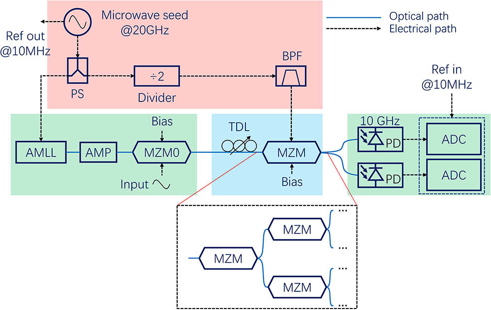
The experimental setup of the channel-interleaved PADC is schematically plotted in Fig. 1. An AMLL (Calmar PSL-10-TT) is used as the optical sampling clock. A synthesizer (Keysight E8257D) outputs a microwave signal at 20 GHz, which is split into two paths. One path is used to seed the AMLL for the generation of a 20 GS/s optical sampling clock, and the other is connected with a frequency divider (RF Bay FPS-2-20) to generate a 10 GHz driving signal. A band-pass filter (SinoSciTe FL2CX10CX02CL12) is used to suppress the harmonics of the 10 GHz signal. The optical sampling clock is amplified by an optical amplifier (AMP, Calmar AMP-ST30) and passes through an MZM (MZM0, Photoline MXIQ-LN-40) with a 40 GHz analog input frequency range for photonic sampling. A microwave generator (Rhode & Schwarz SMA 100 A) is used to generate the signal to be sampled. The 10 GHz driving signal is applied to drive the photonic switch. After photonic sampling, the sampled pulse train with the sampling rate of 20 GS/s is demultiplexed into two channels by a dual-output MZM (EOSpace AX-1x2-0MSS-20), which serves as a photonic switch. As shown in the dotted box in Fig. 1, the sampled pulse train can be easily expanded to multiple channels by a cluster of cascaded photonic switches (i.e., MZMs). In the digitizing of demultiplexed signals, two 10 GHz bandwidth PDs (Conquer PDA-10 G-InGaAs-SM-FA) and two channels of a real-time oscilloscope (Keysight MSOS804 A) are used. A 10 MHz reference output signal of the synthesizer (Keysight E8257D) is used as the reference clock of the oscilloscope during digitization.
Figure 1.Experimental setup of a channel-interleaved PADC with an AMLL for the optical sampling clock and a dual-output MZM for the photonic switch. AMLL, actively mode-locked laser; AMP, optical amplifier; MZM, Mach–Zehnder modulator; TDL, time delay line; PS, power splitter; BPF, band-pass filter; PD, photo-diode; ADC, analog-to-digital converter.
The switching response of the MZM can be expressed by where is the maximum transmittance of the MZM-based photonic switch, and is the temporal period of the optical sampling clock. denotes the extinction ratio of the photonic switch with as the minimum transmittance of the MZM-based photonic switch. The demultiplexing index is defined by where is the phase offset between the sampled pulse train and the driving signal of the MZM. is the modulation index where is the half-wave voltage of the MZM, and represents the amplitude of the driving signal to the MZM.
The transmission model of channel-interleaved PADC[7,15] was investigated, whereas the photonic demultiplexing process is simplified as an ideal pulse response. However, considering the switching response of the MZM as described in Eq. (1), a more explicit model can be derived. The spectrum of digitized data in a demultiplexed channel can be correspondingly evaluated. Here, we define the ratio of the spectrum power of digitized data with and without the photonic demultiplexing, which is described by where and are the digitized signal power with and without the photonic demultiplexing, respectively. Note that the similar derivation can be applied to multiple channels with a cluster of cascaded MZMs (i.e., photonic switches).
Figure 2 shows the simulation result of the dependence of on the amplitude (i.e., modulation index) and phase offset of the driving signal applied to the MZM. The input signal is set to be an 11 GHz single tone. It indicates that the ratio of signal amplitude varies periodically with the phase offset at the period of . If there is a nonzero phase offset, the amplitude of the driving signal is increased to optimize the photonic switching response. When the phase of the driving signal perfectly matches with the optical sampling clock, the amplitude of the driving signal has a minimum value () for the maximum , which is depicted as the crossing point of the dotted and dashed lines in Fig. 2. When the phase mismatch is , there is no switching response, and the parallelization is disabled. Since the extinction ratio and the maximum transmittance (i.e., and ) are given for a specific MZM, the demultiplexing index is the FoM of the photonic switch in the PADC system. By manipulation of both amplitude and phase offset of the driving signal of the MZM, the photonic switching response determined by the FoM [see Eq. (3)] can be correspondingly optimized.
Figure 2.Numerical simulation of the ratio of the spectrum power of digitized data with and without photonic demultiplexing as a function of the modulation index and phase offset.
Note that the phase offset can be implemented by tuning the phase of the driving signal or optimizing the time delay of the sampled pulse train. In the experiment, an optical tunable time delay line (TDL, General Photonics MDL-002) is inserted before the MZM to precisely adjust the phase offset . The bias voltage applied to the dual-output MZM is set at the quadrature bias point. Figures 3(a) and 3(b) depict the power of the digitized data at 11 GHz under different driving powers and phase offset of the driving signal to the MZM. Since of the MZM is about 6.4 V, and the impedance is , the power of the driving signal is set to to achieve a modulation index of 0.5. According to Eq. (3), the demultiplexing index is calculated. The digitized power is depicted in Figs. 3(a) or 3(b) as a function of the RF power (when the phase offset is set to 0) or phase offset (when the RF amplitude is set to ) of the driving signal, respectively. Note that both the digitized power and the calculated are plotted in the decibel (dB) scale. They are in good agreement with the simulated results except for a constant offset, indicating the validation of the theoretical analysis of Eq. (3). When the 10 GHz microwave signal driving the dual-output MZM is turned off, the digitized data represents the experimental results of the PADC without the photonic demultiplexing, and the sampling rate of the oscilloscope is set to 20 GS/s to match the one-channel system without demultiplexing. Figure 3(c) summarizes the measured microwave responses of the PADC with and without photonic demultiplexing. Due to the limited bandwidth of the oscilloscope of , which is lower than the Nyquist bandwidth of 10 GHz of the PADC without photonic demultiplexing, there are two notches near 10 and 30 GHz. However, the notches are significantly recovered because the Nyquist bandwidth of the two-channel interleaved PADC is reduced to 5 GHz for each channel. As a result, the input frequency range of the PADC system can be expanded, and it is possible to get close to the bandwidth of MZM0 (40 GHz) under the sub-sampling principle.
Figure 3.Measured power of the digitized data and the FoM () with different (a) powers and (b) phase offsets of the driving signal to the dual-output MZM. The symbols denote the experimentally measured data, and the solid curves represent the simulated results. (c) Microwave response of the PADC with and without photonic demultiplexing.
In order to verify the feasibility of sampling in the PADC, an 11 GHz single tone with the power of 6 dBm is applied to MZM0. Note that the sampling rate of each demultiplexed channel is 10 GS/s, thus, the sampling rate of each channel in the oscilloscope is correspondingly preset to be 10 GS/s, and the digitized spectrum of the 11 GHz input signal is folded to 1 GHz according to the sub-sampling principle[13]. The spectra of the digitized data in two demultiplexed channels are depicted in Figs. 4(a) and 4(b), respectively. The high-order distortions are suppressed by optimizing the bias voltage of MZM0. The signal-to-distortion ratios (SDRs) of the two channels in Figs. 4(a) and 4(b) are 59.3 and 60.5 dBc.
Figure 4.(a), (b) FFT spectra of the digitized data of an 11 GHz single tone input signal in two demultiplexed channels, respectively. (c) FFT spectrum of the data reconstructed via the time interleaving of two channels.
The data in two channels are time interleaved to reconstruct the digitized data. The sampling rate turns to be 20 GS/s after time interleaving, which folds the 11 GHz input signal back to 9 GHz. The corresponding spectrum is illustrated in Fig. 4(c). Due to the mismatches in the amplitude and phase offset of two channels, there are mismatch spurs appearing in the spectrum of the reconstructed data, leading to an SDR of 32.3 dBc. In order to suppress the spurs, a channel-mismatch compensation algorithm[7] is applied to the digitized data. After the channel-mismatch compensation, the spectrum of digitized data of the 11 GHz signal is depicted in Fig. 5(a). The corresponding SDR is increased to 54.9 dBc, which reaches the maximum value of the EADC and corresponds to an ENOB of 6.9 bits according to the definition[7]. Furthermore, a 31 GHz input signal is also preceded by the same method. The spectrum of the reconstructed data after mismatch compensation is also illustrated in Fig. 5(b). Note that the fast Fourier transform (FFT) spectrum of the digitized data is also folded to 9 GHz due to the sub-sampling principle. The SDR is 51.7 dBc, and the corresponding ENOB is 6.1 bits.
Figure 5.FFT spectra of the reconstructed data after mismatch compensation when the frequency of the input signal to be sampled is 11 and 31 GHz, respectively.
In conclusion, the influence of a photonic switch on a channel-interleaved PADC system is theoretically and experimentally investigated. The FoM of the photonic-switch-based demultiplexing is extracted according to the theoretical analysis. A dual-output MZM is used as the photonic switch, and two demultiplexed channels are digitized in each channel with the optimized FoM. After the data reconstruction and channel-mismatch compensation, the SDRs of the digitized 11 and 31 GHz signals are significantly improved, and the input frequency range of the PADC system is correspondingly broadened.
[18] R. C. Williamson, R. D. Younger, P. W. Juodawlkis, J. J. Hargreaves, J. C. Twichell. 2003 Digest of the LEOS Summer Topical Meetings, MC4.2/22-MC4.2/23(2003).