• Acta Photonica Sinica
  • Vol. 52, Issue 9, 0923003 (2023)
Jianwei CHEN1, Ran HAO1、*, Chunlian ZHAN1, Shangzhong JIN1, Pengju ZHANG2, Xingang ZHUANG2, and Feng FEI2
Author Affiliations
  • 1College of Optical and Electronic Technology,China Jiliang University,Hangzhou 310018,China
  • 2The 41st Research Institute of China Electronics Technology Group Corporation,Qingdao 266555,China
  • show less
    DOI: 10.3788/gzxb20235209.0923003 Cite this Article
    Jianwei CHEN, Ran HAO, Chunlian ZHAN, Shangzhong JIN, Pengju ZHANG, Xingang ZHUANG, Feng FEI. Design Photonic Crystal All-optical Logic Gates Using Machine Learning[J]. Acta Photonica Sinica, 2023, 52(9): 0923003 Copy Citation Text show less

    Abstract

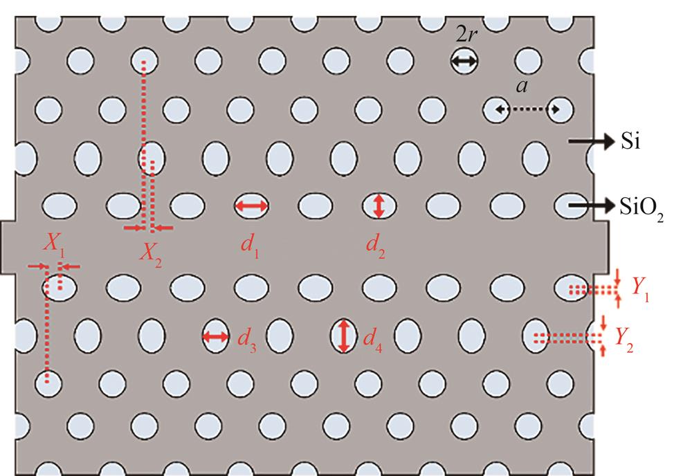
    The all-optical logic gate is the core component of the photonic computer, optical signal processing, and all-optical network. Based on the photonic crystal, the all-optical logic gate has attracted much attention due to its simple structure, low loss, fast operation speed, and small volume. Photonic crystal waveguides can manipulate light for logical operations, which may open up new prospects for photonic computing and optical interconnection networks. However, the design of photonic crystal logic gates is still an iterative process, and the reverse acquisition of geometric structures according to requirements is the key to solving practical engineering problems. To accelerate the performance analysis of photonic crystals and the design of all-optical logic gates, a neural network design of bandgap transmission photonic crystal all-optical logic gates was proposed. In this study, TensorFlow was used as the development framework of the neural network, and a forward performance characterization and inverse structure prediction model of the photonic crystal waveguide was constructed: the forward performance characterization model had 13 fully connected layers, and the total number of parameters trained by the neural network was 197 612, which can realize the timely prediction of the structure of the photonic crystal waveguide to the optical performance; the inverse structure prediction model had 26 fully connected layers, and the total number of parameters trained by the neural network was 155 704, which could reversely design the structure parameters of the photonic crystal waveguide according to the required optical performance, which is helpful to solve practical engineering problems. The Intel Core i9-10940X processor and RTX 3080 Ti graphics card are used for the forward performance characterization and reverse structure prediction network, with training times of 0.2 and 0.36 hours, respectively. The coefficient of determination between the predicted and actual values of the computational neural network was 0.997 for the forward neural network and 0.998 for the inverse network, which shows that the predicted value is very close to the actual value, demonstrating the accuracy of the network. In addition, using the inverse neural network, the structure parameters of the photonic crystal logic gate were successfully predicted according to the required optical properties, such as group index, photonic bandgap, and working wavelength. This logic gate uses gap soliton transmission. When the frequency of the input signal is at the edge of the photonic gap, the output port of the logic gate is nonlinearly disturbed by other input signals. By controlling the frequency and amplitude of the input pulse, the angular frequency displacement caused by the Kerr nonlinearity can be controlled, thus realizing logical operation. The time-domain finite difference method is used to simulate the AND and NOT operations of the all-optical logic gate. The period of the photonic crystal logic gate is 420 nm, and the output port is 70 periods away from the input port. The logic gate performed AND and NOT operations on the Gaussian pulse input signals of“10”and“11”in the time domain, and the output pulse signals of AND and NOT were detected as“10”and“01”, respectively, demonstrating the accuracy of the logic gate. Compared with the input pulse and the output pulse of the AND operation, the pulse width of the input signal was 10 ps, and the output signal was 10.36 ps, with a change of 3.6%. Moreover, when the input pulse intensity was reduced to 1/e, the original pulse width was 5.82 ps, and the output pulse of the logic operation was 5.88 ps, with a change of 1%. This logic gate can achieve stable envelope logic operation in the time domain. The above results show that the use of machine learning to design photonic crystal all-optical logic gates are expected to be applied to the design and optimization of ultra-compact nonlinear optical devices.
    Jianwei CHEN, Ran HAO, Chunlian ZHAN, Shangzhong JIN, Pengju ZHANG, Xingang ZHUANG, Feng FEI. Design Photonic Crystal All-optical Logic Gates Using Machine Learning[J]. Acta Photonica Sinica, 2023, 52(9): 0923003
    Download Citation