Long-distance light detection and ranging (LiDAR) applications require an aperture size in the order of 30 mm to project 200–300 m. To generate such collimated Gaussian beams from the surface of a chip, this work presents a novel waveguide antenna concept, which we call an “optical leaky fin antenna,” consisting of a tapered waveguide with a narrow vertical “fin” on top. The proposed structure (operating around μ) overcomes fundamental fabrication challenges encountered in weak apodized gratings, the conventional method to create an off-chip wide Gaussian beam from a waveguide chip. We explore the design space of the antenna by scanning the relevant cross section parameters in a mode solver, and their sensitivity is examined. We also investigate the dispersion of the emission pattern and angle with the wavelength. The simulated design space is then used to construct and simulate an optical antenna to emit a collimated target intensity profile. Results show inherent robustness to crucial design parameters and indicate good scalability of the design. Possibilities and challenges to fabricate this device concept are also discussed. This novel antenna concept illustrates the possibility to integrate long optical antennas required for long-range solid-state LiDAR systems on a high-index contrast platform with a scalable fabrication method.
1. INTRODUCTION
Integrated silicon(-nitride)-on-insulator (SOI) photonic platforms have matured in the past decades, mainly driven by optical data-communication applications. The technology also shows great potential for more diverse applications in sensing, metrology, and information processing. One of the key characteristics of these platforms is that the waveguides have a high refractive index contrast, resulting in high confinement of the optical modes. This translates to the possibility of making narrow waveguides with small bend radii allowing for dense integration and scaling of optical functionality [1–3].
One of the emerging applications on these platforms is optical phased arrays (OPAs), which are a key element for chip-to-chip free space communication and light detection and ranging (LiDAR) systems [4]. LiDAR systems can be useful in applications such as self-driving cars, bio-metric security, virtual reality (VR), machine vision (e.g., geological surveying, satellite detection), and augmented reality (AR). In LiDAR systems for these applications, a focused beam of light is used to probe the surroundings, map the environment, and track movements [5–13].
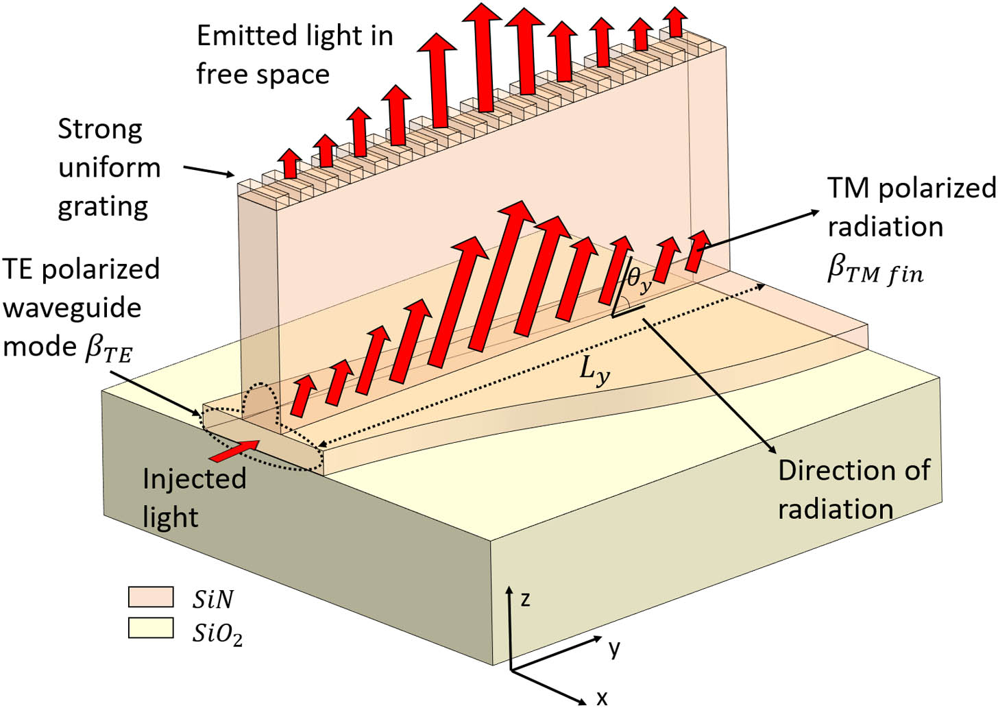
This work introduces a new concept to create an integrated optical antenna on SOI platforms for long-range solid-state LiDAR applications, where apodization of the surface grating is not required but is replaced by a continuously tapered design. The concept illustrated in Fig. 1 shows the proposed geometry to generate a Gaussian beam with a large beam diameter. The motivation to explore this novel geometry is provided in the remainder of the introduction.
Sign up for Photonics Research TOC. Get the latest issue of Photonics Research delivered right to you!Sign up now
Figure 1.3D concept drawing of the proposed antenna structure. A vertical fin on top of a rectangular waveguide can couple the light upward depending on the position of this fin. The radiation strength is proportional to the asymmetry of the structure, defined by the offset of the fin from the center position of the waveguide core. The fin has a strong uniform grating on top to couple the light from the fin to free space, but this grating remains constant (no apodization) throughout the entire antenna design. The core layer tapers underneath the fin structure to maintain the propagation constant of the optical mode, required for emitting a Gaussian beam with a flat phase front. The simulations in this work are carried out with SiN as core and fin material, but the principle also works for Si platforms.
The optical part of a LiDAR system is usually constructed from two main functional subsystems [see Fig. 2(a)]: A ranging engine to determine the distance of the reflector, i.e., using pulses with time-of-flight measurement or a frequency-modulation approach [14,19–21].A beam-steering and beam-forming engine that can shape the beam profile and point it in the right direction. This can be done using either mechanical steering, focal plane arrays, or OPAs [10,22–26].
OPAs are a very promising technique to integrate on the surface of a chip and have the advantage that they can be implemented as a solid-state system. An OPA consists of a 1D (or 2D) array of (or ) antenna elements (optical emitters) periodically arranged along each dimension (and ). Using a 2D array of discrete optical emitters, one can define phases between emitters in both the and directions on the chip surface allowing beam steering in two dimensions, and [see Fig. 3(a)]. This placement is equivalent to 1D OPAs of which each 1D OPA contains optical antennas, which results in phase shifters. This means enabling 2D beam steering requires a vast number of waveguide connections, splitters, and phase shifters to control every antenna output. The 2D approach also drastically increases the number of electrical connections to the optical circuit, like [13,27,28].
Figure 2.(a) Conceptual illustration of a solid-state LiDAR system integrated on a chip surface. An integrated 1D OPA with dispersive antennas is used in combination with a tunable laser to limit the number of input waveguides and phase shifters to . A simplified ranging engine is also illustrated, where a frequency modulation approach can be implemented by using the same laser as a local oscillator and creating a beating frequency with the FM-modulated signal received back from the OPA. This approach is referred to as swept-source LiDAR [14]. The feeding network of these dispersive antennas resembles traditional Butler [15] or Nolen [16] networks from microwave systems. The feeding network can be constructed with a feed-forward Mach–Zehnder mesh circuit [17,18]. (b) To have a large enough Rayleigh range, the near-field beam diameter should be large enough, both in the and directions (illustrated with the “” label on the vertical axis). In other words, the field divergence should be small enough for an adequate resolution [ and , see Fig. 3(a)].
Figure 3.(a) Illustration of an integrated 1D OPA with dispersive antennas on the surface of a chip, consisting of a splitter tree, an array of electro-optic phase shifters connected to an emitting surface, which consists of a dense array of long (in the direction) (apodized) grating coupler antennas. Important parameters such as the divergence angle , the related resolution , and the field of view are visualized. Increasing the aperture size to improves the performance. (b) Detailed illustration of the dispersive antenna elements in the 1D OPA implemented as long apodized grating couplers. The pitch between the emitters (gratings) () should be sufficiently small, for which an HIC is required (enables a high density of antenna elements in the OPA). This implies a very high in-plane aspect ratio of the antenna elements, which makes it difficult to implement a weak grating. The effect of apodization of the grating strength is emphasized by illustrating the undesired exponential decay of an unapodized (i.e., constant parameters along ) grating. The weak part at the beginning of the grating is the most challenging and demanding part of the fabrication, but also the most crucial for a good beam profile.
A sufficient field of view [ and , see Fig. 3(a)] for an antenna array requires a large number of antennas arranged with a sufficiently small pitch, and (Fig. 3). For example, to allow steering of the beam to an angle of from the vertical on the axis (), for a wavelength of 1550 nm, the antenna pitch in the direction should not be larger than 1.7 μm [13]. The high-index contrast (HIC) of Si or SiN waveguides is suited for this purpose, as dense integration of a large number of elements on a small surface area is possible in these systems (as illustrated in Figs. 3 and 2). This is incompatible with the spacing required to feed all optical and electronic signals to every optical emitter (grating coupler) in a 2D OPA [13,27,28].
To mitigate these scalability issues for 2D OPAs, more simple 1D OPAs with dispersive antennas [as illustrated in Figs. 2(a), 3(a), and 3(b)] can also be used to perform 2D beam steering. These emitting surfaces consist of long dispersive optical antennas (as opposed to antennas for 2D OPAs). The dispersive nature of the optical antennas (such as diffraction gratings) enables beam steering in the direction () with a variation of the wavelength , which can be centrally controlled for all long antennas of the 1D OPA. Using wavelength steering reduces the number of required antenna elements (and, thus, phase shifters, routing waveguides, and electrical connections), which makes it easier to position the antennas with a small pitch [7,10,13,22,29].
For practical LiDAR applications, the optical beams need to be projected over a sufficiently large distance [see Fig. 2(b)] (i.e., automotive LiDAR, free space communication, geological mapping, spacecraft, machine vision) [5–7,9,10,13]. If we want to probe far-away objects (i.e., ), the aperture size needs to be in the order of 30 mm. This follows from the Rayleigh range of a Gaussian beam, with being the beam radius (the operating wavelength we target is μ). This would determine the required on-chip aperture size (i.e., the length of the grating) to be . Since an aperture of this size would truncate the beam at 86% of the power of a full Gaussian profile, the performance of a LiDAR system can be improved by increasing the aperture size to suppress sidelobes and other imperfections in the far field. To capture 99% of the power in the Gaussian beam, the aperture size can be increased to [see Figs. 3(a) and 3(b)] [13,30].
While an HIC waveguide helps to minimize , making such a long optical antenna comes with challenges in such a platform. The propagating mode in the waveguide will be very sensitive to geometrical perturbations [3]; therefore, it is difficult to implement very weak, well-controlled periodic gratings in the guiding structure to create out-of-plane grating couplers. One would have to resort to very small perturbations with subnanometer precision and reproducibility, which are inherently hard to fabricate reliably. In other words, any grating in a waveguide with HIC will be too strong, resulting in beams with a waist that is too narrow (and, thus, a large divergence and low resolution) for these practical LiDAR applications. Adding a collimating lens above the chip can help, but this will reduce the angular scanning range along [ on Fig. 3(a)] when we sweep the wavelength.
In this publication, we side-step this problem to define a weak grating. We present an alternative concept for an optical antenna that mitigates many of the scalability issues of long gratings (see Section 2). In this new antenna, we adapt the concept of lateral leakage devices to explore a novel geometry that gives us continuous control over the power radiating away from a guided mode in the waveguide (see Fig. 1) [31–33].
First, we present a short overview of the current state-of-the-art grating-based antennas and their limitations in Section 2. In Section 3, we discuss possible mechanisms to create leaky wave antennas in mm-wave technology, where non-periodic antennas are presented as a fundamental alternative to periodic structures such as gratings and how we can implement a similar concept in dielectric optical waveguides. Next, the device concept is discussed in Section 4, where the cross section is discussed in more detail and the relevant parameters that can be used to tune both the leakage rate and propagation constant are presented. These parameters are swept in simulation to construct a design space, and the sensitivity to possible deviations is analyzed. In Section 5, the design space is utilized to construct a full antenna from a targeted power profile and propagation constant. The simulation results of the designed antenna derived in Section 5 are presented in Section 6, where both the resulting power profile and far-field are analyzed.
2. LONG (WEAK) GRATING COUPLERS WITH HIGH-INDEX CONTRAST: CURRENT METHODOLOGIES
Directly defining gratings in the waveguide core on either Si or SiN platforms reports beam diameters well below the target of 30 mm [34–36], and the longest reported near-field beam diameter (3 mm) in literature (to our knowledge) uses a sidewall corrugated SiN waveguide [37].
The fundamental challenge to create long (weak) optical antennas using periodic perturbations in an HIC material system (i.e., long gratings) is illustrated by Bruck and Hainberger in Ref. [38], where an analysis of the optimum spot-size (beam diameter) in relation to the grating etch depth is analyzed in a low index-contrast system with increasing thickness of an HIC layer. The study shows that reducing the index contrast of the geometrical perturbations is crucial to increase the beam diameter, and this can be achieved by using a thinner layer of HIC material.
To overcome this problem, one can fabricate a weak grating with an HIC material using a gap between the waveguide core and the perturbations to diminish the strength of the grating. This is demonstrated in Refs. [39–41]. Another mechanism to decrease grating strength with these overlays employs a lower index contrast material (SiN) on the silicon waveguide to define the grating overlay, as demonstrated in Refs. [42–44]. Both with or without a separation layer, all these mechanisms report beam diameters well below the target of 30 mm and even below the sidewall corrugated devices presented in Ref. [37].
If we want this grating antenna to emit a Gaussian beam profile rather than the exponential decay obtained from a conventional grating with uniform strength [see Fig. 3(b)], one has to resort to apodization of the geometrical perturbations creating the grating [34,37,45]. This technique gradually increases the perturbation strength (i.e., etch depth) of the grating from 0 to a maximum value, creating an increasing index contrast along the length of the grating. This has the effect of increasing the strength of the grating, increasing the coupling from a guided mode to free space, and creating a Gaussian beam shape [Fig. 3(b)].
The long double-layer SiN antennas reported by Raval et al. [37] (with the largest near field beam diameter in literature) also implemented the apodization technique (to our knowledge, over the longest length found in literature). The two layers of nitride have a geometrical perturbation that increases with the distance along the antenna. It can be noticed that the antenna presented in Ref. [37] needs a perturbation depth up to 10 nm, starting from 0 nm, within the first 1000 μm of the device. This implies an increase in the order of 10 pm/μm, which is challenging on a large scale with high yield since a silicon atom has a van der Waals radius of 210 pm. Increasing the length of the antenna will even result in more gradual apodization curves, making it even harder to realize. This shows that apodization for longer beams would require more gradual and precise control over the apodization than what can be reliably fabricated.
Because both the Si and SiN material systems (or combinations) exhibit fundamental challenges to achieve antenna lengths (and corresponding beam widths) in the order of 30 mm and demand unfeasible control on fabrication due to the apodized periodicity (especially in the beginning of the emitter where the grating should be very weak), it can be interesting to investigate an alternative vertical coupling mechanism to decouple the apodization (grating strength) from the out-of-plane grating coupler.
3. LEAKY WAVE ANTENNAS WITHOUT PERIODICITY
In mm-wave technology, the concept of traveling wave antennas (or leaky wave antennas) has been known for decades [46–49]. This class of antennas uses a traveling wave on a guiding structure as the main radiating mechanism. This usually relies on the knowledge that a “fast wave” (meaning the phase velocity is higher than the speed of light in vacuum) allows phase matching to occur between the propagation constant of the waveguide and free-space propagation at a certain angle [49]. The most basic example of a mm-wave fast-wave antenna implementation is an air-filled metal waveguide with a slot opening in the top surface, acting as an antenna aperture [46–49].
A grating coupler antenna is an example of a “slow” leaky wave antenna, where a slow wave () has a fast spatial harmonic mode due to a periodic perturbation [49]. This is the only way to achieve vertical emission out of a dielectric optical waveguide.
It is possible to arrive at an intermediate scheme without resorting to a direct periodic perturbation of the guided optical waveguide mode, where a dielectric radiating channel can be implemented using dielectric slab waveguides in the waveguide cladding leading to leaky conditions similar to that of a fast wave antenna in mm-wave. Because the -vector of a TE-polarized slab mode in the cladding of a ridge waveguide is larger than the -vector of the fundamental TM-polarized waveguide mode, phase matching allows the guided mode to couple to the TE-polarized slab mode propagating at a certain angle. These modes radiate away from the waveguide core in the lateral direction, hence the name lateral leakage [31–33].
The leaky behavior can be geometrically tuned using the waveguide width because the coupling to these slab modes physically originates from interference between two radiating discontinuities on the left and right side of the waveguide cross section (where the overlap of longitudinal field components yields coupling between the guided TM-polarized mode and the radiating TE-slab modes). This mechanism can alter the leakage from extremely high values (decay lengths of only a few wavelengths) to almost zero (no leakage). The waveguide width values where this high and low lateral leakage occurs are called the anti-magic and magic widths, respectively [31–33].
It has to be noted here that, in order to achieve any sort of vertical coupling from this slab to free space, a periodic perturbation still would be required because the -vector of the slab modes still is situated below the light cone. So this mechanism only couples light from the waveguide core to the slab in the cladding, but the geometrical parameters that influence the coupling strength are all much easier to control. The grating that can then couple light to free space can be designed to be very strong and uniform (unapodized), which is much easier to achieve than a weak grating. In other words, we can avoid the use of precise periodic features that require subnanometer fabrication precision. This exact technique was actually used to observe the lateral leakage in Ref. [33].
4. VERTICAL LEAKY FIN ANTENNA CONCEPT
Inspired by this lateral leakage mechanism, we propose a novel antenna concept where we rotate the waveguide core and the slab 90°. The in-plane “slab” now becomes a vertical “fin,” and the leakage is no longer lateral (in the plane of the chip) but out of the plane of the chip, at an angle from the vertical. The guided mode is now the TE-polarized mode in the waveguide core region, coupling to the TM mode of the vertical slab (from here on referred to as fin), as illustrated in Fig. 4. Note that there is only a single fin on top, in contrast with the lateral leakage waveguide, which can leak in both directions. This will have a significant impact on the mechanism that we use to control the leakage rate.
Figure 4.Illustration of the film mode matching modeling configuration of the vertical leaking structure. The top and bottom boundary condition is implemented as a transparent boundary condition (TBC), while the sides are implemented as perfect electric conductors (PECs). The structure is analyzed for different values of the waveguide core width and the offset. The core thickness, , and the width of the fin have the same value for all simulations. The transparent boundary condition on the top surface is equivalent to continuing the physical fin toward infinity, guiding power outside the simulation window at the radiation angle . Simulations in this work use SiN as core and fin material, but the principle also works for Si platforms.
The structure resembles the cross section of a groove antenna used in mm-wave technology with metallic waveguides (either filled with dielectric or air). Here, a vertical fin (in this context sometimes referred to as “stub”) is placed on top of a rectangular waveguide. When this fin is off-centered with respect to the waveguide core, the asymmetry will cause the guided mode to become leaky [46,50–53]. For the optical implementation of this antenna and the simulations presented here, we chose SiN as the guiding layer, but the antenna could also be implemented in Si or other materials used for making dielectric optical waveguides.
A. Control of the Leakage Rate
Generally, a leaky mode has a complex effective index which can be written [54] as which we rewrite as This allows us to extract the leakage rate, which in this context we call radiation strength (which can be intuitively interpreted as the rate at which the TE-polarized mode in the waveguide core couples to the TM polarized mode in the fin as is explained later), as follows: While this complex propagation constant follows directly from rigorously solving Maxwell’s equations fully in this cross section of lossless materials, an intuitive way of understanding this leakage behavior is to see it as a coupling between a lossless propagating waveguide mode and off-axis slab modes in the fin, which we call the radiating modes. When the structure is fully symmetric, the guided TE mode in the waveguide core and the radiating TM mode in the fin have different symmetries. Therefore, their modal overlap is zero, and they do not couple (see Fig. 6). Changing the position of the vertical fin relative to the waveguide core center (referred to as the offset) breaks this symmetry, which results in a coupling between the TE-polarized core mode and TM-polarized fin mode (meaning increases with a larger offset). This coupling is enabled by the fact that both modes have a field component along the axis (the propagation direction of the waveguide), which is strongest near the corners where the fin meets the core, so the two modes can couple if their overlap integral becomes non-zero. Indeed, as the symmetry of this component is different for the TE and TM modes, the coupling cancels out completely when the fin is centered on the waveguide core. However, once the fin is off-center, the coupling increases, and this can be very accurately controlled. Note that the component, and therefore the magnitude of this effect, become stronger when the core and fin material has a high refractive index contrast with the surrounding cladding
This leakage principle makes it possible to define a cross section where the offset monotonically maps to the radiation strength of the structure, giving the possibility to vary the cross section along the propagation direction from a fully bound mode to a strongly radiative mode, increasing along the length of the antenna.
B. Control of the Propagation Constant
Another requirement for antennas in an OPA is a constant emission angle over the entire length of the antenna to guarantee a flat phase front. This requires a constant phase velocity of the waveguide structure. Otherwise, the emitted wavefront will be curved (either converging or diverging), which would be equivalent of having a smaller emitting surface, negating the advantage of having a long antenna.
The phase velocity is expressed as the real part of the propagation constant of the guided waveguide mode, where . As the Kramers–Kronig relations couple the real and imaginary part of , a change in is induced whenever (the radiation strength of the mode) changes, so we need to add a second degree of freedom in the cross section to compensate for this change in . This can be done by changing at the same time as changing the offset, creating a 2D design space spanned by the offset and the core width. In theory, other parameters such as or could be used for the same purpose, but we chose the two parameters that are most convenient to control in planar fabrication processes. The other parameters, including the width of the fin, are kept constant over the entire antenna length.
C. Simulation of the Design Space
The design space of the cross section was simulated at a wavelength μ using a film-mode matching (FMM) technique with transparent boundary conditions. The FMM-solver used here was REME, specifically developed at RMIT to study lateral leakage behavior of ridge waveguides [31]. When we use transparent boundary conditions on the top and bottom of the cross section, the FMM-solver is able to determine the of a guided mode with . We simulated the cross section on a parameter grid of discrete design coordinate pairs to determine both and , and we used a bi-variate smooth spline interpolation algorithm from the scipy package to interpolate the results. The result is a 2D design space for the radiation strength, plotted as a color map in Fig. 5, with overlayed contours.
Figure 5.Radiation strength of the cross section in dB/cm, plotted with contours visualized. For a given constant phase constant of the antenna, design values have to be selected from one contour. For these simulations μ, , and .
In this simulation, transparent boundary conditions are used to allow power to leak away from the simulation window. The FMM technique is one of the few techniques that allow for true transparent boundaries along one lateral axis, not requiring perfectly matched layers, which always have some residual reflections [31]. This means that for our simulations we assume that the fin extends indefinitely and light does not (yet) couple to free space. In real fabricated devices, the height of the fin needs to be finite, and the coupling from the fin to free space will require a periodic structure (as mentioned in Section 3). It has to be noted here that the need for a periodic structure is not fundamentally required since the light is already propagating vertically in the fin, as opposed to the lateral leakage in the slab. This means a tilted top surface at Brewster’s angle could also be used here. Since this approach would lack a strong angular dispersion required for wavelength steering (as is discussed later; see Section 6.B), the most obvious method of coupling the light from the fin to free space is a strong uniform (blazed) grating designed to divert all incident light to the first diffraction order. There is no need for apodization in this grating because the beam profile is determined by the leakage rate from the waveguide to the fin (i.e., by the waveguide/fin offset, see Section 5).
For a smooth Gaussian-shaped emission profile, we want a continuous design with increasing leakage rate but exhibiting a constant in the longitudinal direction ( direction). So we can select one of the contours in Fig. 5 to give us a mapping of the core width and offset to radiation strength of the cross section for a given propagation constant .
Figure 5 shows that, for each given value of , increasing the offset results in a higher radiation strength (). The maximum absolute value of the offset increases for larger values of , but it maintains a similar relatively.
This behavior can be intuitively explained by examining the imaginary part of the longitudinal component () of the TE mode in the cross section on the top surface of the waveguide (i.e., the bottom aperture of the fin) shown in Fig. 6.
Figure 6.Imaginary part of longitudinal field component . (a) Zero offset (lossless symmetric structure). (b) Maximum symmetry breaking by increasing the offset to the maximum value. The red curves show sampled on the aperture of the vertical fin (the top surface of the waveguide) indicated in the figure with a white dotted line. Breaking the symmetry of the structure results in an increasing overlap with the slab mode of the fin because the mode profile becomes highly asymmetric in the waveguide.
In the perfectly symmetric case [, Fig. 6(a)], the anti-symmetric nature of in the guiding structure causes a cancellation effect in this mode coupling because the overlap with the TM mode in the fin is zero. When the offset increases, the symmetric profile of the fin will have an increasing overlap with the guided mode of the structure, and coupling to the fin is possible. This coupling increases in strength as has the largest values near the unperturbed waveguide edges [Figs. 6(a) and 6(b)].
D. Sensitivity Analysis
Because the design space was interpolated using a bi-variate spline algorithm, we also have access to the local derivatives. These can learn us something about the theoretical sensitivity to certain fabrication parameters such as and the offset. The derivatives are plotted in Fig. 7, together with the used for the antenna design (see Section 5) in this work.
Figure 7.Values of the partial derivatives from the spline interpolation used to create Fig. 5 to determine a prediction of the sensitivity to fabrication variation in both and the offset. The contour with is highlighted in each plot. (a) Variation of with the offset in . (b) Variation of with the width in . (c) Variation of with the offset in . (d) Variation of with the width in .
This analysis reveals the fundamental advantage of using this approach rather than the apodization of a periodic structure. As pointed out in the introduction, the most crucial and challenging part of the antenna design is at the start of the propagation, where radiation has to be weak. Making such a weak grating requires very precise control on fabrication and will be sensitive to a deviation from the target design value.
If we consider Figs. 7(c) and 7(d), we see that for low values of the offset (and thus ) the sensitivity to a geometrical deviation of both the design parameters, offset and , is low. This implies that this cross section is less sensitive to fabrication variation of the design parameters in the weak regime at the start of the antenna. The sensitivity increases if we follow the contour determining the antenna design parameters for a given , meaning that higher values of will be more susceptible to any deviation. This means the relative “error” will be always small, and the most significant deviations will be found toward the end of the antenna, where most optical power has already radiated out of the waveguide. This built-in robustness in the weak radiation regime is a clear advantage over apodization methods used on periodic structures.
Figures 7(a) and 7(b) show the deviation of (and thus ) with a change in offset and . A similar trend with the sensitivity of to the design parameters can be observed in Fig. 7(a). The value of will change the least at the start of the antenna in the weak radiation regime (low values of offset). This is also the section of the device with most of the power still present in the guiding structure. As light propagates along the contour, sensitivity increases. Figure 7(b) reveals that the sensitivity of to will be similar for all values on the design contour.
When we follow the for the design wavelength of 1.55 μm, the value of remains constant, as can be seen in Fig. 8. If the values of the index contour are used at another wavelength, the contour will not produce constant values. We solved the modes for the cross sections on the with μ and μ to analyze the sensitivity of the radiation angle to the wavelength. As can be seen in Fig. 8, the values remain relatively constant when the offset , but when we increase the value of , and thus the propagation constant , the corresponding emission angle starts to deviate from its initial value. This will result in a slightly converging phase front for shorter wavelengths and a diverging phase front for longer wavelengths. But, as we will show in Section 5, the offset only goes to this region toward the very end of the antenna design, where most power has already radiated from the device and the impact on the center of the beam is limited. Still, to compensate for this effect, we could consider unlocking one or more additional design variables, such as the width of the fin .
Figure 8.Corresponding values with increasing offset following the for the antenna design with μ. Ideally, all values remain constant with increasing offset, but at wavelength deviating from the design wavelength, we see a deviation of the initial value of when the offset increases. The deviation is stronger at higher values of the offset.
To design an antenna with a target power output profile, the first step is back-calculating the radiation strength at each position along the antenna (which would be the apodization function when using a periodic perturbation as discussed in the introduction).
We start from a desired output power profile of the antenna, which in the context of LiDAR will be a Gaussian beam as mentioned in the introduction. We use a 100 μm discretization to define this profile with segments (profile[1] to profile), which means we can determine the required radiation ratio per segment as illustrated in Fig. 9.
Figure 9.Discretization of the antenna in segments to calculate required from for each segment. By requiring , meaning that all incoming (normalized) power is radiated, the entire radiation profile can be back-calculated.
The antenna should dissipate all input power, , which implies . This means the last segment should radiate all incoming power from the previous antenna segment, meaning or . This determines , so we can determine and continue this process for all preceding antenna segments. Because , we now know the required radiation strength . The output of this process is illustrated in Fig. 10, where Fig. 10(b) shows the resulting for the Gaussian power profile with plotted in Fig. 10(a).
Figure 10.(a) Target Gaussian power profile () for antenna, centered at 15 mm. This profile function is sampled with a step of 100 μm, so each point profile[n] resembles the power emitted by 1 segment of the discretization. (b) Output of the back-calculation illustrated in Fig. 9. This function is used to determine the cross-sectional parameters at each coordinate.
As mentioned before, the antenna requires a constant propagation constant for a constant emission angle along the propagation direction . This means we can select one of the contours from the interpolated design space for a specific antenna design with given , shown in Fig. 11. These curves were obtained by sampling points with from the interpolated design space (Fig. 5). On these sampled points, a polynomial was fitted for [Fig. 11(a)] and a uni-variate spline was fitted for [Fig. 11(b)]. The function offset has a very steep start, illustrating the robustness of cross sections with low radiation strength.
Figure 11.(a) Fitted polynomial to sampled points on with (μ) from Fig. 5. (b) Fit of offset to corresponding values on sampled , . If from Fig. 10(b) is used as an input, with (b) we can determine the required offset at each position, after which we can determine the required width with (a) to ensure constant .
Combining the curve [Fig. 10(b)] with the function obtained in Fig. 11(b), , results in the required offset at each coordinate of the antenna [], plotted in Fig. 12(a). With and the function [Fig. 11(a)], we can determine the accompanying width of each cross section [] shown in Fig. 12(b). The offset increases quasi-linearly with for the largest part of the device.
Figure 12.(a) Resulting tapering function from Fig. 11(a) using as input. (b) Resulting offset function from Fig. 11(b) starting from target function Fig. 10(b). The small bump is caused by numerical errors in the bi-variate fit near the low-loss regions because the loss increases very gradually with the offset for small values.
With the antenna design functions from Fig. 12, the cross section of each coordinate is determined. The resulting structure is conceptualized in Figs. 1 and 13. The fin is kept uniform and straight over the entire antenna length, while the waveguide core is tapered according to Fig. 12(b) in such a way that the offset changes according to Fig. 12(a). As mentioned in Section 4.C, a strong uniform grating on top of the fin is still required to couple the light from the fin to free space. No apodization is needed because the radiation strength is continuously tuned by the tapered waveguide position underneath.
Figure 13.Top view of an array of the proposed antenna geometry, which now replaces the fabrication sensitive gratings used in Figs. 2 and 3. Note that the high aspect ratio of the antenna is required for dense integration along the axis.
It should be noted that the strong grating on top should be sufficiently far away from the guiding structure, meaning the fin would require a thickness of at least 2 μm. While fabricating such a fin is still not trivial, the fact that it is uniform over the entire antenna length makes it easier to optimize a fabrication process specifically for this structure. We believe this is an improvement on the scalability of long-distance optical antenna designs since the core layer and fin structures can be fabricated in separate steps and the design is inherently robust to deviations of the offset between the fin and core.
6. SIMULATION OF THE ENTIRE ANTENNA
A. Power Profile at Design Wavelength
The geometry of the antenna design with determined in Section 5 is constructed within the REME eigenmode propagation engine [31]. Using the design functions from Fig. 12, the corresponding cross section for each segment is determined, and the corresponding modes are calculated using the FMM algorithm with transparent top and bottom boundary conditions. The REME mode solver calculates the overlap between all sections to determine mode couplings between each segment, and we launch the TE-polarized waveguide mode (μ) from the left ().
We then monitor the leaky TM component of the fields (), just before it hits the transparent upper boundary (i.e., just below where we would position a strong grating as illustrated in Fig. 1).
The extracted 2D power profile () in Fig. 14(a) was constructed using 100 μm discretization segments, which means the number of cross sections to be analyzed is in the order of 300. The fin and core layers are visualized to help with the interpretation of the plot. Note the very distorted aspect ratio: the device is approximately 1.5 μm wide in the direction, while 30 mm long in the direction.
Figure 14.(a) Top view of a 3D simulation result of the antenna design (μ) presented in Section 5. In this simulation, segments with a length of 100 μm were used to discretize the design, and then FMM with transparent boundary conditions was used to determine the modes of each segment. The core layer and fin are visualized to aid the interpretation of the field plot. Note the high aspect ratio of the simulation window. (b) 1D view of the power on the black dotted line, together with the target Gaussian [Fig. 10(a)]. Due to the discretization, a small ripple is introduced on the simulated power profile. The bump caused by numerical errors is also visible here.
The data on the black dotted line represented in Fig. 14(a) normalized to peak power were used to create a 1D power profile plot. The larger discretization size introduces a ripple in the power profile, which is strongest at the peak of the profile (). The target Gaussian from Fig. 10(a) normalized to peak power is also shown to see if they match. At most positions, the target profile is approached very well (the peak position matches quasi perfectly), even with this larger discretization size.
The strongest deviation from the target profile is in the beginning just before . This is related to numerical artifacts and errors that are introduced by the two subsequent curve-fitting procedures. The first one is used in Section 4.C to interpolate the 2D design space. This generates enough samples to select an with sufficient precision from the design space. On this sampled contour, functions are again fitted in Fig. 11, as described in Section 5. The effect of these numerical errors can also be seen by a bump in the curve in Fig. 12(b) just before . This shows the offset has to increase linearly to obtain a perfect Gaussian power profile, but the numerical fitting errors cause a deviation from this linear increase. This is not a fundamental limitation, and it could be further fine-tuned by sampling the design space in more detail in the low-leakage regime.
B. Far Field and Wavelength Dependence
To determine the quality of the phase profile, we sample the field on the aperture of the fin and calculate the far field. As mentioned before, these simulations do not include the grating structure on top of the antenna (it is replaced by a transparent boundary), so we simulate the far field in an infinitely high fin structure in the direction. As a comparison, we calculate the far field of the target intensity Gaussian [Fig. 10(a)] with a perfect phase ramp radiating at the analytically calculated phase matching angle , which determines the direction of radiation in the fin (see Fig. 1).
This angle can be determined as Here, is the effective index of the TM polarized slab mode in the fin, and is the propagation constant of the antenna. For the design wavelength of the antenna (μ), we find The results are shown in Fig. 15(a). The simulated field on the aperture matches the target field quite well and agrees with the phase-matching angle. There is a small difference in peak angle (almost negligible, this can be attributed to numerical artifacts), but the far-field of the sampled field has the same full width at half-maximum (FWHM) value as the discretized version. This shows that the phase profile of the simulated field in the aperture almost approximates a perfect phase ramp and deviations can be attributed to the discretization of the design with 300 cross sections.
Figure 15.(a) Calculated far field at μ from simulated field in the aperture, compared to the ideal target far field (target Gaussian with perfect phase ramp). (b) Simulated wavelength dependence of far-field angle. The FWHM value is indicated for each wavelength to assess the wavelength dependence of the divergence.
Since both the numerator and denominator in the analytical expression for are susceptible to dispersion, will also be wavelength dependent. This is not a problem, as we wish to use the wavelength to perform beam steering along the axis anyway. We simulated the antenna designed for μ at other wavelengths and calculated the corresponding far-field profiles. The results are shown in Fig. 15(b). When the wavelength increases, so does the direction of radiation , but only with a relatively small value (). This is insufficient for wide-angle wavelength steering but reveals robustness in terms of performance when deviating from the design wavelength. We also see that the beam divergence angle increases 5%–15% for the longer and shorter wavelengths, which corresponds to the nonuniform profile plotted in Fig. 8.
To enable wavelength steering, a low-reflection blazed diffraction grating without any required apodization could be implemented on top of the fin (as mentioned in Section 4.C). This grating will have a much stronger angular dispersion than the antenna, allowing the beam to change direction () significantly with wavelength steering [see Fig. 3(a)]. The -vector of the grating should be determined such that the wavelength of 1.55 μm is diffracted upward (), requiring a grating period in the order of The robustness of the radiation angle to the wavelength also means that a misalignment between core and fin in fabrication would not affect the incidence angle of the emitted beam toward the strong grating on top.
7. CONCLUSION AND OUTLOOK
Long-range LiDAR requires Gaussian beams with a wide waist, and it is not trivial to tailor such emission profiles in an HIC waveguide platform with an OPA antenna. We need the high contrast material system because a small antenna pitch is necessary, but conventional techniques utilizing apodized periodic perturbations require impossible precise fabrication that does not scale well to larger antennas. Therefore, it would be beneficial to avoid periodic, grating-like structures for the apodization of the radiation profile and instead use a continuous design.
Since leaky wave antennas without periodicity are only possible in “fast” guiding structures () and dielectric optical waveguides only guide “slow” waves (), an intermediate radiation channel can be engineered in the form of a vertical slab waveguide called a “fin.” This is inspired by the same principle as lateral leakage where power can leak from a guiding structure laterally. Since no periodic grating is used to construct the emission intensity profile, we eliminate unfeasible fabrication requirements.
The proposed cross section of our leakage-based antenna is based on a single geometrical parameter (the offset of the fin relative to the waveguide core) to tune the radiation strength. The core width of the waveguide, , is then changed accordingly to maintain the propagation constant and ensure a constant angle of radiation to end up with a collimated beam. This leads to a design that has a continuous tapered waveguide core where both and the offset to the fin change simultaneously (see Figs. 1 and 13).
The proposed structure can be fabricated in two separate steps, i.e., one defining the waveguide layer and the other defining a subsequent deposition of the fins. This would require the alignment of two different masks, with relaxed alignment conditions for both the and directions. This tolerance to alignment originates from the fundamental robustness of the cross section to the offset in the most crucial part of the design, the beginning of the antenna. The device also exhibits robustness to changes in wavelength, meaning that the far-field radiation angle is not strongly dependent on the wavelength and remains constant for wavelengths other than the design wavelength μ.
The simulations in this work use a transparent boundary condition where a strong uniform grating should be placed to diffract the light from the fin into free space and to provide a strong wavelength dependence for steering in the direction.
This device concept comes with its own fabrication challenges but has built-in tolerance and robustness that provide the scalability required for precise long-range LiDAR systems. The main fabrication challenge to overcome is the height of the fin, more specifically the high aspect ratio. This must be sufficient to decouple the leakage profile from the diffraction at the top grating. The fin, therefore, needs to be patterned in a thick layer of a high-index material (here, silicon nitride) with sufficiently vertical sidewalls. The fin profile also needs to be very uniform along the length of the antenna and between the many antennas in a large OPA. For this reason, we kept the fin geometry as simple as possible to facilitate the process development. Alternatively, the width of the fin could be used as an additional design parameter by tapering the fin along the length of the antenna, i.e., to perform a first-order compensation of the wavelength dispersion that gives rise to a slightly curved wavefront (and beam widening) for longer and shorter wavelengths.
At this point, we did not yet include the strong uniform grating in the simulations (a transparent boundary condition was used instead). Due to the large length of the device (in these simulations ), including the grating in the entire device was not computationally feasible at the time. One possibility is to use the FMM simulation output presented in this work and sample the vectorial field components on the surface of the TBC. Using this field as input, the near-field of the grating can be obtained by performing an finite-difference time-domain (FTDT) method in a much smaller simulation window (it can severely be limited in size in the dimension). The far field from the grating can then again be obtained using a plane wave decomposition analysis.
Even though it is much easier to fabricate a strong uniform grating compared to the apodized gratings with a very weak radiating section, it is still not trivial. The efficiency of the device is reliant on the efficiency of the periodic grating on top, but the leakage-based antenna provides a mechanism to avoid apodization of the grating teeth. The grating ideally should have no reflections and only a single diffraction order, which introduces its own challenges in fabrication. A strong grating will be less sensitive to fabrication variation, but it is still challenging to have a uniform structure on this length scale. For instance, it could be implemented as a blazed grating or a volume-phase holographic grating.
We believe that this device presents a promising alternative to conventional periodic gratings to facilitate scalable 1D OPAs with dispersive antennas as an emitting surface for long-distance solid-state LiDAR integrated on a chip.
Acknowledgment
Acknowledgment. We thank Thach Nguyen and Arnan Mitchell for the use of the FMM-solver (REME) to simulate the cross section and propagation of leaky modes [31].
[3] R. Baets, A. Z. Subramanian, S. Clemmen, B. Kuyken, P. Bienstman, N. Le Thomas, G. Roelkens, D. Van Thourhout, P. Helin, S. Severi. Silicon photonics: silicon nitride versus silicon-on-insulator. Optical Fiber Communications Conference and Exhibition (OFC), 1-3(2016).
[8] S. A. Miller, C. T. Phare, Y.-C. Chang, X. Ji, O. A. J. Gordillo, A. Mohanty, S. P. Roberts, M. C. Shin, B. Stern, M. Zadka, M. Lipson. 512-element actively steered silicon phased array for low-power lidar. Conference on Lasers and Electro-Optics, JTh5C.2(2018).
[9] M. Watts. Towards an integrated photonic LIDAR chip. Imaging and Applied Optics, AIW4C.1(2015).
[15] Y. Zhang, Y. Li, P. Liu, Z. Zhang. Dual-beam antenna array using integrated butler feeding network. International Symposium on Antennas and Propagation (ISAP), 1-2(2019).
[25] X. Zhang, K. Kwon, J. Henriksson, J. Luo, M. C. Wu. A 20 × 20 focal plane switch array for optical beam steering. Conference on Lasers and Electro-Optics, SM1O.3(2020).
[26] C.-W. Baek, S. Song, C. Cheon, Y.-K. Kim, Y. Kwon. 2-D mechanical beam steering antenna fabricated using MEMS technology. IEEE MTT-S International Microwave Sympsoium Digest, 211-214(2001).
[49] Z. N. Chen, J. H. Choi, T. Itoh, D. Liu, H. Nakano, X. Qing, T. Zwick. Beam-scanning leaky-wave antennas. Handbook of Antenna Technologies, 3, 1698-1732(2016).
[51] P. Lampariello, F. Frezza, H. Shigesawa, M. Tsuji, A. Oliner. Guidance and leakage properties of offset groove guide. IEEE MTT-S International Microwave Symposium Digest, 731-734(1987).