Leopold Virot1,2,3,4, Laurent Vivien1, Jean-Marc Fedeli2, Yann Bogumilowicz2..., Jean-Michel Hartmann2, Frederic Boeuf5, Paul Crozat1, Delphine Marris-Morini1 and and Eric Cassan1|Show fewer author(s)
This paper reports on high-performance waveguide-integrated germanium photodiodes for optical communications applications. 200 mm wafers and production tools were used to fabricate the devices. Yields over 97% were obtained for three different compact photodiodes (10 × 10 μm and intrinsic region width of 0.5, 0.7, and 1 μm) within the same batch of three wafers. Those photodiodes exhibit low dark currents under reverse bias with median values of 74, 62, and 61 nA for intrinsic widths of 0.5, 0.7, and 1 μm, respectively, over a full wafer. Responsivities up to 0.78 A∕W at 1550 nm and zero bias were measured. Zero bias operation is possible for 25 and 40 Gbps with receiver sensitivity estimated to -13.9 and -12.3 dBm, respectively.
Optical communications are already well established for medium to long-range applications such as access, metro, and long haul, making use of discrete III–V components offering high performances but at high costs. With the increasing bandwidth needs for developing communication applications—including cloud computing and storage—mobile multimedia services, high-definition content diffusion, and short communication links tend to be limited by the copper line throughput. Then optical data transmission is needed to overcome this limitation. However, to enable the dissemination of such products, costs must be reduced and production volumes and yields drastically increased. Silicon photonic integrated circuits are now seriously considered, and active optical cables are using those circuits for data center backplane connections, reducing the cables’ management complexity and power consumption. Complementary metal oxide semiconductor (CMOS) manufacturing facilities offer all the tools needed to fabricate such silicon photonic circuits. Still, this implies the development of complex integrated devices, with performances comparable to III–V compound materials counterparts, at a lower cost. To address this challenge, high-performance active devices including modulators and detectors integrated on silicon have already been reported [1–22], as well as passive devices to connect them. Fabricating integrated high-efficiency sources remains tricky and/or costly, despite the demonstration of hybrid InP-based [22–26] and Ge lasers [27,28]. The main concern for active devices is to offer the lowest possible power consumption while maintaining their high performance in terms of bandwidth, efficiency, and loss. Germanium-based photodiodes were widely developed in the last decade [1–15], and now offer cutting-edge performance, directly concurencing their III–V counterparts. Where Ge photodiodes take advantage is in their integration with other silicon-on-insulator (SOI) components: Ge heteroepitaxy on Si offers a simple integration scheme at low cost, with high throughput, and is fully compatible with CMOS processes and tools. Despite the lattice mismatch between Si and Ge, very good crystalline quality Ge layers using various growth processes have been reported [29–36]. Both vertical [2–5,11,12,14] and lateral [9,10,15] PIN photodiode configurations, as well as metal-semiconductor-metal (MSM) structures [6–8,13], have been studied and fabricated for photodetection. Despite their very simple structure and fabrication, MSM photodetectors often suffer from large dark current due to the low Schottky barrier on Ge. Moreover, low bias operation (below 1.2 V for advanced CMOS-driven photonic circuits) does not allow efficient carrier collection and high bandwidth. Thus, even if PIN photodiode fabrication remains more complex compared to MSM, they should fulfill all the requirements for next-generation photonic circuits.
This paper reports on the development of lateral PIN germanium photodiodes integrated with silicon waveguides on 200 mm SOI substrate using standard microelectronic tools and processes. Our aim was to develop the most efficient photodiodes in terms of raw performance (bandwidth, responsivity) and power consumption, at the lowest cost. Those devices exhibit performance compliant with 40 Gbps optical communication systems. Very high optical bandwidth (over 50 GHz), as well as responsivity up to at a wavelength of 1550 nm, have been achieved at zero bias. Those photodiodes also present a very low dark current (typically 25 nA at reverse bias), while offering very simple integration within a standard CMOS process flow. The design and fabrication will be detailed as well as the DC and AC characteristics, complemented by simulations and data transmission performance evaluations.
2. DEVICE DESIGN AND FABRICATION
A. Photodiode Integration Scheme
The integration of the photodiode with Si waveguides must remain as simple as possible, to minimize the costs and increase the robustness, without neglecting the performance of the device. The main considerations that have been taken into account in order to fabricate such photodiodes are presented hereafter.
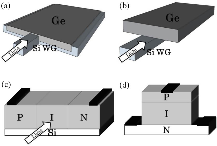
First, we need to couple the light from a SOI waveguide to the photodiode. Two schemes are possible and led to very good coupling efficiency and resulted in high performance in terms of bandwidth, responsivity, and/or dark current. The light can be coupled either evanescently from the waveguide to the upper Ge layer or directly from the waveguide to Ge by butt coupling, as shown in Figs. 1(a) and 1(b), respectively. The Si waveguide is designed to be single mode at wavelength of 1550 nm. The chosen waveguide height and width are 220 and 500 nm, respectively.
Figure 1.Waveguide-coupling configurations: (a) butt coupling and (b) evanescent coupling. PIN junction configuration: (c) lateral and (d) vertical.
Using the RSOFT beam propagation method (BPM), we have simulated the absorption efficiency at a wavelength of 1550 nm in a Ge layer with the following parameters: 10 μm width, 20 μm length, and 350 nm thickness. For the butt-coupling scheme, we have included a 50 nm thick Si seed layer, mandatory for Ge growth. For the same absorption efficiency of 96%, lengths of 10 and 17 μm are required for butt coupling and evanescent coupling, respectively, as shown in Fig. 2. The absorption length can be reduced for evanescent coupling by optimizing the Ge layer thickness, whereas it has little or no influence in the case of butt coupling. For a fixed Ge thickness of 350 nm, at a given absorption efficiency of 96%, the device capacitance is then 1.7 times higher for evanescent coupling, increasing the RC (resistance-capacitance product) time constant of the device.
Figure 2.Absorption efficiency and device capacitance for evanescent and butt-coupling configurations, assuming intrinsic region width of 1 μm and Ge height of 350 nm.
The second point is the PIN junction configuration. It can be either vertical or lateral [Figs. 1(c) and 1(d)]. Both have yielded similar results. The intrinsic region width or height can be controlled by ion implantations or by Ge growth with in situ doping, for the lateral and vertical configurations, respectively.
B. Intrinsic Region Design
The design of the intrinsic region will determine the performance of the photodiodes in terms of bandwidth and responsivity. From previous considerations, butt coupling has been chosen to have a compact device with reduced capacitance. The thickness of the Ge layer is not an optimized parameter in our case, simplifying the process control. Since 96% of light should be absorbed over a 10 μm propagation length, such integration is a good trade-off between device capacitance and absorption efficiency. In order to keep the integration simple, the lateral PIN junction is preferred. Therefore the metallic contacts on both -type and -type Ge regions can be performed using a single etching step. Two etch depths would by contrast have been required with a vertical PIN diode configuration. The intrinsic region width (noted ) must at least match the Si waveguide width, to limit the absorption in the doped regions, which lead to carrier recombination, degrading the intrinsic responsivity. Fig. 3 shows the simulated light absorption in the intrinsic region for three values of (0.5, 0.7, and 1 μm), from which the maximum theoretical responsivity is estimated and reported in the inset of the figure.
Figure 3.BPM simulation of light absorption in the intrinsic region of a lateral PIN photodiode for a 350 nm thick Ge layer in a μ cavity, butt coupled to a Si waveguide (). The intrinsic region width is set at 0.5, 0.7, and 1 μm. The inset reports the maximum responsivity for those conditions at 1.55 μm wavelength.
The frequency response of PIN photodiodes is mainly driven by the transit time across the depletion layer and the RC time constant induced by the global capacitance and resistance of the device. The transit time is directly obtained by the ratio of the depletion length to the carrier drift velocity : and the RC time constant is defined by where is the equivalent resistance of the photodiode circuit and is the junction capacitance assuming no “package” capacitance, which is defined as follows: with the Ge dielectric constant and the area of the junction. To get a rough estimate of the photodiode maximum theoretical bandwidth, we will assume at first that the depletion length is equal to : the intrinsic region is supposed to be fully depleted, and the active dopant concentration is high enough so that the space charge region will not be extended under a few volts reverse bias. Moreover the -type and -type doped region are assumed to have constant doping level with abrupt profiles at the edges of the intrinsic region. Following the methodology presented in [37], the transfer function of the photodiode can be analytically calculated to obtain the frequency response with contributions from both the RC and transit time parts. The sheet resistance of the photodiode has not been taken into account, and only a 50 Ω load resistance is considered. Taking into consideration the dimensions of the Ge layer (which is 10 μm long and 350 nm thick), the maximum opto-electric bandwidth is reported in Fig. 4 as a function of the intrinsic region width. As seen from this graph, the bandwidth is dominated by the transit time if the intrinsic region width remains over 150 nm. The highest reachable bandwidth, without degrading too much absorption efficiency, is obtained when the intrinsic region matches the waveguide width (here 500 nm) and is estimated to be around 70 GHz.
Figure 4.Photodiode maximum theoretical bandwidth.
Another point essential in the achievement of low power consumption and highly sensitive receivers is the dark current. Germanium has very narrow (direct and indirect) bandgaps. Thus, reverse biasing PIN junctions leads to an increase of the dark current, mainly because of trap-assisted tunneling (low electric field) or band-to-band tunneling (high electric field). To maintain high signal-to-noise ratio (SNR), independently of the bandwidth, dark current has to be reduced to its minimum. This can be achieved with very good crystalline quality germanium as well as with a low electric field inside the junction (by applying a low reverse bias or increasing the intrinsic region width). However, the latter can lead to a reduction of the drift velocity of the photogenerated carriers, degrading the bandwidth. Yet, only good epitaxy process conditions control can allow very low dark current, and no particular care in design is necessary. Three photodiode designs were chosen with different intrinsic region widths. Those devices will be called A, B, and C for equal to 0.5, 0.7, and 1 μm, respectively, and are described in Table 1 with their expected performances.
Photodiode L=10μmhGe=0.35μm
A
B
C
wi (μm)
0.5
0.7
1
Junction capacitance Cj (fF)
1
0.7
0.5
Responsivity (A/W)
0.91
0.96
0.99
−3dB opto-electrical bandwidth (GHz)
70
50
35
Table 1. Theoretical Performances of the PIN Ge Photodiodes
The photodiodes and passive structures (fiber couplers and waveguides) have been fabricated on 200 mm SOI wafers with 2 μm buried oxide (BOX) and 220 nm upper Si layer using CEA-Leti clean room facilities. The single-mode strip waveguides () as well as the grating couplers were fabricated by 193 nm deep-UV lithography followed by dry etching of the Si layer down to the BOX. An 800 nm thick layer was then deposited and polished down to 700 nm by chemical–mechanical polishing (CMP). μ cavities were defined and and Si layers were etched at the end of the waveguide, leaving roughly 50 nm of Si at the bottom of the cavity, as illustrated in Fig. 5. Ge was selectively grown (with GeH4) into the Si cavity by the reduced-pressure chemical vapor deposition (RPCVD) technique. In order to accommodate the lattice mismatch () between Ge and Si, a thin Ge buffer layer was grown at low temperature (400°C) followed by a thicker layer grown at higher temperature (750°C), yielding a higher growth rate, a smoother surface, and some defect curing. To avoid faceting of the Ge layer inside the Si cavity, the Ge was overgrown outside of the cavity, which also has the benefit of reducing the threading dislocation density (TDD) [32]. When the photodiode will be reversed biased, the threading dislocations will serve as generation centers, thus increasing the dark current. To further reduce the TDD, the selective epitaxial growth was followed by short thermal cycling under H2 [38]. Finally, a CMP step was used to recover a flat surface and reduce the Ge layer thickness down to around 350 nm, as shown by the cross-sectional transmission electron microscopy (TEM) image in Fig. 6. A layer was deposited prior to the ion implantation step to protect the Ge layer and limit dose loss during activation anneals. A self-alignment process was used to ensure a good definition of the intrinsic region centered on the Si waveguide. Intrinsic regions with three widths (0.5, 0.7, and 1 μm) have been fabricated. -type and -type regions were implanted with phosphorus and boron, respectively. Rapid thermal annealing (RTA) was used to activate the dopants. A capping layer was deposited, and the contacts on the doped Ge regions were fabricated by etching μ via holes down to the Ge-doped regions. Ti/TiN was then deposited prior to filling with and a last CMP step. Electrodes were fabricated by depositing and then patterning a Ti/TiN/AlCu metal stack. Three 200 mm wafers were processed within the same batch with the same conditions. This allows analysis of homogeneity over a wafer as well as wafer-to-wafer uniformity. Some statistical results and the best device performances are then reported.
Figure 5.Schematic cross-sectional view of the final photodiode structure. Light coming from the waveguide is injected into the intrinsic region of the Ge photodiode perpendicularly to the schematics.
In this section, characterization of the three types of photodiodes (A, B, and C) will be presented. The experimental results will be compared to theoretical expected characteristics, and we will discuss and try to explain the discrepancies with the help of simulations.
A. DC Measurements
Dark current was first measured as a function of the applied bias for the three PIN photodiodes described previously (A, B, and C), this over the full wafers. Yield results are provided in Table 2.
Wafer 1
A
B
C
−1V
85 nA
66 nA
68 nA
−2V
296 nA
182 nA
186 nA
Yield (functional diodes)
99.2%
100%
100%
Wafer 2
A
B
C
−1V
74 nA
62 nA
61 nA
−2V
261 nA
167 nA
160 nA
Yield (functional diodes)
99.73%
100%
100%
Wafer 3
A
B
C
−1V
112 nA
80 nA
71 nA
−2V
451 nA
219 nA
195 nA
Yield (functional diodes)
97.85%
99.73%
100%
Table 2. Dark Current Median Values over Full Wafers (373 dies per wafer) for the Three Types of Photodiodes
The yield displayed is the ratio of the number of photodiodes exhibiting the current-voltage characteristic of a diode to the total number of photodiodes. The median is more representative than the average since the latter will be degraded by very leaky photodiodes (with dark current in the range of several microampere). The best photodiodes have then been selected for detailed measurements. Table 3 shows the best dark current and corresponding current densities obtained for the three types of photodiodes. Such dark currents are in the range of the best reported values for Ge PIN photodiodes, and close to their III–V counterparts. The lowest dark current value is obtained for C-type photodiodes and was equal to 6 nA under .
A
B
C
Current (nA)
Current densitya (mA/cm2)
Current (nA)
Current densitya (mA/cm2)
Current (nA)
Current densitya (mA/cm2)
W 1
32
91.4
18
51.4
19
54.3
W 2
25
71.4
9.5
27.1
17
48.6
W 3
27
77.1
9.2
26.3
6
17.1
Table 3. Best Dark Current and Dark Current Density Values under Reverse Bias for the Three Wafers and the Three Photodiodes
A full current-voltage characteristic is shown in Fig. 7 for the three photodiodes measured on the same die. They exhibit very good rectifying characteristics. Series resistances were extracted from the 0.8–1.5 V region of the curves; values ranged from to . It is clear from I–V measurements that our photodiode leakage shows a strong dependence on the electric field. Indeed, the dark current directly increases with increasing bias and/or reducing intrinsic region width (the smaller , the stronger the electric field). To guarantee the best SNR, the dark current must remain as low as possible. A low reverse bias is thus preferred as long as it does not degrade the responsivity and the frequency response of the photodiode.
Figure 7.Typical dark current characteristics of photodiodes A, B, and C (, 0.7, and 1 μm, respectively).
In order to evaluate the responsivity of the photodiodes, the coupling losses of the grating couplers were measured using a test structure composed of two grating couplers connected by a wide Si waveguide (2 μm width and 220 nm height) assuming no propagation losses along the waveguide. Since the grating couplers were optimized for TE polarization, a polarization controller was used at the output of the laser, and the optical power at the output of the polarization controller was measured to be 544 μW. The coupling losses at a wavelength of 1550 nm were extracted, and the optical power at the input of the photodiode was then estimated to be around 110 μW. The photocurrent does not increase with increasing reverse bias. The electric field inside the depletion region is high enough to extract all the photogenerated carriers even at zero bias. The responsivity at 1550 nm increases from 0.52 to when goes from 0.5 to 1 μm, with for the μ diode.
B. AC Measurements
The capacitances of the photodiodes were measured at 1 MHz using a calibrated LCR meter. The capacitance evolution with applied reverse bias is shown in A, B, and C, respectively. From for the three types of photodiodes. At , capacitances were measured to be , , and for photodiodes A, B, and C, respectively Fig. (8). From PIN junction simple theory, it is estimated that if the doping concentrations are high enough and symmetric in the -type and -type doped regions, with abrupt profiles, the space charge region will not extend that much (few nanometers) with reverse bias. However, clear voltage dependence is shown here, meaning that the intrinsic region is not fully depleted under low reverse bias, which is also due to the nonabrupt doping profiles.
Opto-electrical characterization measurements were performed using a 1550 nm wavelength laser modulated up to 50 GHz and a network analyzer. Prior calibrations were performed to correct the contributions from cables and the RF probe. The response given by the network analyzer is expressed in decibels, which is calculated as follows: where is the photocurrent generated in response to the optical incident power at a frequency . The “1” at the denominator is expressed in A/W. is thus related to an electrical power, and the -3 dB level gives the opto-electrical bandwidth, which is not the optical bandwidth. In order to get the optical bandwidth, has to be divided by 2. The optical bandwidth can then be obtained. Measurements were fitted using a single pole RC filter, and the opto-electrical as well as the optical bandwidth were extracted or extrapolated from this fit. The measured frequency response at 1 V reverse bias is presented in Fig. 9(a) for the three studied photodiodes together with the fit. The frequency response starts to rise above 40 GHz due to the noise floor level of the network analyzer. In order to keep a good fitting accuracy, the experimental points beyond 40 GHz were not taken into account during the regression. The bias dependency of the opto-electrical bandwidth of the photodiodes is shown in Fig. 9(b). The maximum bandwidth is measured to be around 45 GHz, and is estimated to 62 GHz for device B and over 90 GHz for device A. Table 4 summarizes the measured parameters for the three photodiodes.
Figure 9.(a) Photodiode frequency response at bias. For clarity purposes, the curves for photodiodes A and C were artificially shifted by and , respectively. (b) opto-electrical bandwidth function of the applied reverse bias for the three photodiodes. A, B, and C type photodiodes have , 0.7, and 1 μm, respectively.
The maximum bandwidth is greater and the responsivity lower than the theoretical ones. It corresponds to a reduction of the effective intrinsic region width, leading to a smaller transit time and also to a decrease of the absorption efficiency due to higher overlapping between the optical modes and the doped regions. To investigate this effect, process simulations were run, in particular ion implantation and annealing steps. Monte Carlo ion implantation simulations were performed with Silvaco ATLAS software. Those simulations were calibrated with secondary ion mass spectrometry (SIMS) profiles to ensure the validity of the results. Good agreements were found between the simulated and measured 1D profiles. Using those calibrated profiles, it was possible to simulate the ion implantation in 2D for the -type and -type doped region definition, for the three types of photodiodes, and the doping profiles along the junction are shown in Fig. 10. Besides, phosphorus is known to be diffusing into germanium [39–42]. With our annealing conditions, phosphorus diffused during the activation annealing step, further reducing the effective intrinsic region width. Diffusion mechanisms of phosphorous are still not yet well understood, and the lack of parameters in Silvaco ATHENA prevented us from accurately matching SIMS profiles after annealing.
Figure 10.TCAD simulated implantation profiles for the three designed intrinsic region widths, obtained by cross section along the dashed line shown in the inset of the figure.
Based on the previous results, receiver sensitivity has been evaluated. For this study, an on–off keying (OOK) modulation format is considered. Assuming that the probability function for optical noise can be approximated by a Gaussian, and according to [43], the bit-error-rate (BER) can be expressed by , or the factor, represents the SNR at the receiver decision circuit in voltage or current units and can be written [43] as where and are the averaged values of “1” bits and “0” bits, respectively, and and are the standard deviations of “1” bits and “0” bits, respectively. By means of Eq. (5), the factor can be obtained for a given BER. Since we are interested in the ultimate sensitivity of the receiver, we expect that the light levels coming on the photodiode are quite small. We can then assume without introducing significant errors. Thus, the minimum detectable power level (or sensitivity) is given by with the internal responsivity of the photodiode in A/W, the combined root-mean-square (rms) noise current of the photodiode and receiver [trans impedance amplifier (TIA)], and the ratio of power received in the “0” state to that in the “1” state. For the OOK modulation format, . The frequency response of the photodiode is taken into account by applying a penalty to the responsivity; i.e., if the bandwidth is 40 GHz, then the responsivity will be divided by 2. Making use of Eq. (7), it is possible to estimate the sensitivity of the photodiode at given BER and bit rate. The contributions to the rms noise current of the photodiode are the noise, which is negligible at high frequency, the thermal or Johnson noise , and the shot noise due to statistical fluctuations in the incident photon flux , which are expressed as follows: where is the electron charge, is the dark current, is the photocurrent, is the bandwidth, is the Boltzmann constant, is the temperature, and is the equivalent resistance of the photodiode. The Johnson noise will be affected by the load impedance of the photodiode, which when coupled with a TIA is the input impedance of the amplifier. Assuming the shunt resistance of the photodiode is much higher than the load and series resistance, we can write , which should be dominated by . However, the thermal noise of this resistance is already accounted for in the input referred noise of the TIA; thus the thermal noise term has not been included. According to best commercially available TIA for 40 Gbps, the typical value of the rms noise current is of the order of , giving roughly 2.85 and 2.37 μA at 25 and 36 GHz bandwidth, respectively.
In the following analysis, the BER is fixed to and the corresponding value is 7, evaluated from Eq. (5). For 25 Gbps applications, the type B photodiodes exhibit the highest responsivity at 25 GHz under zero bias; consequently they will have the greatest sensitivity. The sensitivity of the receiver using photodiode B is computed as a function of the global rms noise current (including both the photodiode and TIA contributions). The sensitivity will be limited by the TIA noise, giving a maximum sensitivity of . At reverse bias, type C photodiodes exhibit the highest responsivity at 25 GHz. Including the dark current to the shot noise with a typical value of 61 nA at , the sensitivity is still limited by the TIA but increases to . Further increase of the reverse bias leads to sensitivity at with photodiode C. In any case, the front end noise will limit the performance of the photodiodes, and a very low noise amplifier will be needed to increase the sensitivity of the receiver.
For 40 Gbps operation, type A photodiodes yield the highest responsivity at zero bias, leading to sensitivity. At reverse bias, type C photodiodes will offer the greatest sensitivity, i.e., . Pushing the reverse bias to will only increase sensitivity to .
The lack of low noise TIA for data rates over 10 Gbps limits the maximum sensitivity of Ge PIN-based receivers. Assuming an ideal PIN photodiode with maximum theoretical responsivity at 1550 nm of at zero bias (without dark current), maximum TIA limited sensitivity will be around . To achieve sensitivities over this value, with actual TIA, the only way is to increase the use of avalanche photodiodes (APDs). However APDs require high bias, thus increasing the power consumption, but also limiting its integration with CMOS-based drivers.
4. CONCLUSION
We have demonstrated the integration of Ge photodiodes on Si at the wafer scale using selective epitaxial growth of Ge with very good yields over three 200 mm wafers. The lateral butt-coupling configuration of the PIN photodiodes allowed simple process integration with limited steps and good robustness. The fabricated photodiodes exhibited responsivity ranging from 0.52 to at 1550 nm. The dark currents reported here are the lowest achieved for such a photodiode configuration, proving the good crystalline quality of the epitaxial Ge layer, with only 6 nA for the best device, and 61 nA for the median value over a wafer, under . Zero bias operation led to optical bandwidth over 50 GHz, enabling 40 Gbps data transmission with very low power consumption. Using commercially available TIA characteristics, the sensitivity of a receiver based on presented photodiodes, biased at , has been estimated to be and for data rates of 25 and 40 Gbps, respectively, for a BER of .
[8] K. Ang, S. Zhu, M. Yu. High-performance waveguided Ge-on-SOI metal–semiconductor–metal photodetectors with novel silicon–carbon (Si:C) Schottky barrier enhancement layer. IEEE Photon. Technol. Lett., 20, 754-756(2008).
[9] J. Wang, W. Y. Loh, K. T. Chua, H. Zang, Y. Z. Xiong, S. M. F. Tan, M. B. Yu, S. J. Lee, G. Q. Lo, D. L. Kwong. Low-voltage high-speed (18 GHz/1 V) evanescent-coupled thin-film-Ge lateral PIN photodetectors integrated on Si waveguide. IEEE Photonics Technol. Lett., 20, 1485-1487(2008).
[11] S. Klinger, M. Berroth, M. Kaschel, M. Oehme, E. Kasper. Ge-on-Si p-i-n photodiodes with a 3 dB bandwidth of 49 GHz. IEEE Photon. Technol. Lett., 21, 920-922(2009).
[25] S. Stankovi, R. Jones, M. N. Sysak, J. M. Heck, G. Roelkens, D. Van Thourhout, A. Abstract, V. Iii. Hybrid III–V/Si distributed-feedback laser. IEEE Photon. Technol. Lett., 24, 2155-2158(2012).
[30] J. M. Hartmann, A. M. Papon, P. Holliger, G. Rolland, T. Billon, M. Rouvière, L. Vivien, S. Laval. Reduced pressure—chemical vapor deposition of Ge thick layers on Si (001) for microelectronics and optoelectronics purposes. MRS Proc., 809, B4.3.