Abstract
In this work, a soliton mode-locked erbium-doped fiber laser (EDFL) with a high-quality molecular beam epitaxy (MBE)-grown topological insulator (TI) Bi2Se3 saturable absorber (SA) is reported. To fabricate the SA device, a 16-layer Bi2Se3 film was grown successfully on a 100 μm thick SiO2 substrate and sandwiched directly between two fiber ferrules. The TI-SA had a saturable absorption of 1.12% and a saturable influence of 160 MW/cm2. After inserting the TI-SA into the unidirectional ring-cavity EDFL, self-starting mode-locked soliton pulse trains were obtained at a fundamental repetition rate of 19.352 MHz. The output central wavelength, pulse energy, pulse duration, and signal to noise ratio of the radio frequency spectrum were 1530 nm,18.5 pJ, 1.08 ps, and 60 dBm, respectively. These results demonstrate that the MBE technique could provide a controllable and repeatable method for the fabrication of identical high-quality TI-SAs, which is critically important for ultra-fast pulse generation.Two-dimensional (2D) materials, also named layered materials[1], define a new material morphology where single or few layers of atoms gather together in one direction, while in the other two directions they keep uniform and crystal-like expansions. With the reduction in physical dimension, 2D materials bring totally different and exciting new energy band structures, possessing unique optical and electronic characteristics[2,3]. One of the most dramatic things is that they could be used as ultra-fast passive saturable absorbers (SAs), the modulators, or mode lockers for fiber lasers[4–9]. Usually, they are of interest because of their flexibility in fabrication, wideband absorption, and ultra-fast light–matter interactions.
Initialized from graphene in 2009[10–14], a considerable amount of 2D materials have been investigated in ultra-fast fiber lasers, including topological insulators (TIs: [15–17], [18,19], [20]), transition metal dichalcogenides (TMDs: [21,22], [23–25], [26], [27], [28], [29], [30]), black phosphorus[31–36], MXenes[37,38], bismuthene[39,40], etc. Among them, TIs own intrinsic direct bandgaps of , bridging the gapless graphene and materials with large gaps like TMDs. The small bandgap makes them good candidates for wideband optical modulators from visible to mid-infrared regions. For instance, both silica fiber[17,41–43] based and fluoride fiber[44] based mode-locked lasers operated between 1.0 and 3.0 μm have been realized with TI .
There are many physical and chemical methods used to synthesize TIs and other kinds of 2D materials, which could be summarized into two branches: the top-down exfoliation and the bottom-up growth[45]. Among them, mechanical exfoliation (ME) and solution processing (SP) methods are most widely adopted. However, ME methods have low yield and produce only micro-sized irregular flakes. Similarly, SP methods like liquid-phase exfoliation are also uncontrollable, making a fabricated SA an integral effect of tiny flakes with different sizes and directions. It is noteworthy that all of these traditional methods need either dry or wet transferring processes for desirable fiber SAs, which have to rely on water, chemical, or organic solvents[45]. During these processes, 2D materials are also susceptible to extra contamination and may bring degradation. In contrast, thin TI films grown epitaxially on or substrates are controllable[46,47], possessing high quality by maintaining pristine morphology and crystallinity[48]. Recently, we have used the P-scan method[49] to investigate the nonlinearities of different layered continuous films grown by the molecular beam epitaxy (MBE) technique, providing a deep look into their surface states and saturable absorptions[50]. Besides, we also demonstrated that a controllable SA could be achieved by changing the material thickness or excitation wavelength.
Sign up for Chinese Optics Letters TOC. Get the latest issue of Chinese Optics Letters delivered right to you!Sign up now
In this work, we report on the soliton mode-locking operation of a ring-cavity erbium-doped fiber laser (EDFL) at 1.5 μm. Firstly, a high-quality film with a large area of and a thickness of 16 nm was grown epitaxially on a substrate. Secondly, it was divided into small pieces and sandwiched directly between two fiber ferrules to fabricate the fiber SA. Finally, it was inserted into the EDFL, and self-starting soliton mode-locking operation at 1530 nm was obtained with a pulse width of and a repetition rate of 19.352 MHz. Since the aforementioned growing and transferring processes for TI-SAs were controllable and repeatable, it is important to clarify that they are appropriate for quantity productions of high performance identical SAs for ultra-fast mode-locked fiber lasers.
The high-quality film was prepared by the MBE technique as introduced in previous work[46]. In this work, a 100 μm thick plate was selected as the substrate. It had a size of . The growing time for one layer was . Thus, to obtain a 16-layer film, the total time spent was .
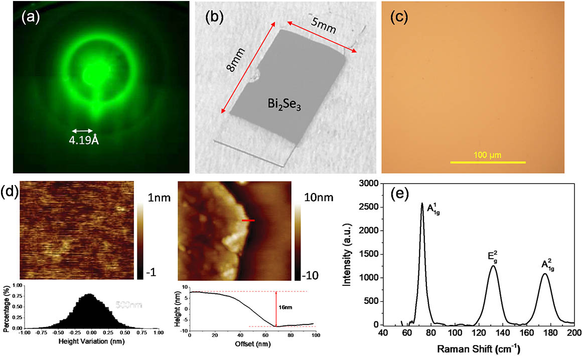
Figure 1 provides the morphological and structural characteristics of the grown film. Figure 1(a) depicts the monitored reflection high-energy-electron diffraction (RHEED) pattern with a lattice constant of 4.19 Å(1 Å = 0.1 nm). As shown in Fig. 1(b), the prepared sample had a metallic luster with a size of regardless of the blocked area by clamps. Figure 1(c) displays an optical microscopic image of the film with uniform color contrast and absence of defects. It was found that this film had excellent continuity over the whole grown region. Using an atomic force microscope (AFM), the film’s surface morphology and thickness were characterized. As shown on the left of Fig. 1(d), the surface over an area of was smooth and followed with the normal distribution law. As shown on the right of Fig. 1(d), the measured thickness of the film was 16 nm. Considering the thick value of per layer, thus the layer number was calculated to be . Furthermore, Raman spectroscopy was also used to identify the material structure of this layered film. The corresponding result is depicted in Fig. 1(e). Obviously, there were three intensity peaks located around 72, 130, and , ensuring the high purity of the film. It is important to note that the MBE technique is highly controllable in designing the film’s layer number. In order to measure the recovery time of film, a two-color pump–probe measurement[51,52] was performed. When pumped at 400 nm and probed at 690 nm, a fast relaxation time of was measured, showing the 16-layer film’s potential for ultra-fast light modulators.

Figure 1.Characterization of films on substrate. (a) RHEED pattern. (b) Visible photo. (c) Optical microscopic image. (d) Surface morphology (left) and thickness (right) measured via AFM. (e) Raman spectrum.
In the experiments, the film on the 100 μm substrate was divided mechanically and butt coupled between two fiber ferrules to fabricate the fiber SA. Such a thin thickness guaranteed small mode field mismatch loss at the second ferrule, where the laser light coupled back into the fiber core. This method eliminated the possibility of SA degradation in the material transferring process.
Figure 2 depicts the experimental setup of the ring-cavity EDFL. The lasing was provided by a 30 cm length of single-mode erbium-doped fiber (EDF) pumped by a 980 nm laser diode (LD) via a 980/1550 nm wavelength division multiplexer (WDM). The single-mode EDF had an absorption coefficient of at 980 nm, with a dispersion coefficient of at 1550 nm. A polarization-independent isolator (ISO) was used to ensure counter clockwise laser propagation. The laser output was extracted from the 10% port of a fused fiber optical coupler (OC) after the WDM. Before the TI-SA, a polarization controller (PC) was used to adjust the laser polarization. The pigtails of these optical components were made of standard single-mode fiber (SMF28). In addition, another piece of SMF28 was added into the laser cavity to enhance the nonlinearity. The whole cavity length was about 10.6 m with a calculated negative dispersion of . The negative dispersion was very beneficial to the generation of soliton pulses.
Figure 2.Schematic setup of ring-cavity EDFL.
To analyze the output characteristics, we used a digital oscilloscope (bandwidth 1 GHz), a radio frequency (RF) spectrum analyzer with a high-speed InGaAs optical detector (bandwidth 5 GHz), a power meter, and an optical spectrum analyzer (with a spectral resolution of 0.05 nm). In addition, a second harmonic autocorrelator was used to measure the pulse width.
Figure 3 illustrates the characteristics of the as-prepared fiber TI-SA. As shown in Fig. 3(a), a divided small piece of was transferred onto a ferrule connector (FC)/angled physical contact (APC) ferrule. Therefore, the laser light in the fiber core propagated through the film vertically. In this work, a home-made balanced twin-detector method was adopted to investigate the nonlinear transmission of the TI-SA. A fiber laser provided the injection light, which delivered laser pulses at 1550 nm. The measured results are depicted in Fig. 3(b). Meanwhile, a nonlinear function is used to fit these measured data, in which , , and represent the modulation depth, the nonsaturable loss, and the saturable power, respectively. is the peak power of injected pulses. is the peak power-dependent transmission. As can be seen in Fig. 3(b), the fiber SA had a modulation depth of 1.14% and a nonsaturable loss of 71.2%. The fitted was 80 W, which corresponded to a saturable intensity of .
Figure 3.Characteristics of fiber SA. (a) Photo of piece on fiber ferrule. (b) Nonlinear transmission curve.
By adjusting the pump power and the PC position properly, mode-locked pulses were generated successfully, and the output was summarized in Fig. 4. Typical soliton bunch pulses were measured as in Fig. 4(a), when the mode locking started at the pump power of 122 mW. The time interval between adjacent bunches was 51.67 ns, which matched with the cavity round time. The inset shows the pulse intensities were almost the same, and the soliton number in a single bunch was three. Once pump power and PC were fixed, the positions of internal pulses remained unchanged as well, which was a typical characteristic of soliton bunches. Figure 4(b) plots the measured spectrum. The spectrum had its central wavelength of 1530 nm and 3 dB bandwidth of 2.8 nm. Weak Kelly sidebands of soliton pulses located at 1520 and 1541 nm were also observed. Since there were no interferences between soliton pulses in a bunch, no spectral modulation was observed. But, when they clustered close enough, slight spectral envelope modulation was observed, like in Ref. [53]. Figure 4(c) shows the measured pulse autocorrelation (AC) trace of the soliton pulses, which was well-fitted with a profile. The full width at half maximum of the AC trace was 1.67 ps, corresponding to a pulse width of 1.08 ps. Then, the time–bandwidth product of these soliton pulses was calculated to be 0.388.
Figure 4.Soliton pulses characteristics. (a) Pulse train. (b) Optical spectrum. (c) Autocorrelation trace. (d) Average output power and soliton energy versus pump power. (a)–(c) were measured at a pump power of 122 mW.
In Fig. 4(d), the average output power of the soliton pulse train was measured as a function of the pump power. Two dotted lines were plotted, illustrating the mode-locking regions. “A” was for the pump increasing process, while “B” was for the pump decreasing. A pump power of 60 mW started the continuous wave operation of the laser. As the pump power was increased to 122 mW, a stable self-starting mode locking was observed as discussed before. The mode-locking operation maintained by merely increasing the pump to its maximum or by decreasing it to 72 mW. Soliton numbers in bunches at different pump powers were recorded and depicted in Fig. 4(d). No significant hysteresis phenomena were observed, like in Ref. [16]. Due to the limited pump power, a soliton number of up to six was observed. Thus, we were able to calculate output soliton energy at different pump powers, as plotted in Fig. 4(d). Obviously, there was an upper limitation of output energy of about 18.5 pJ, which corresponded to a maximum intra-cavity energy of 185 pJ. Once the pulse energy reached the limitation and by further increasing the pump power, the soliton number would be added by one; meanwhile, the pulse energy decreased. This phenomenon was in accordance with the soliton area theorem[54]. In a laser cavity with net negative dispersion, the peak power limiting effect usually causes multi-pulsing of quantized solitons[19,55]. To overcome the soliton bunches or multi-pulsing, cavity dispersion management could be introduced[23].
When the pump power was in the range of 72–86 mW, single soliton mode-locking operation could be obtained. Figure 5(a) plots the measured pulse train. Although the nonsaturable loss of the TI-SA was large, the single soliton mode-locking operation could still work steadily for 24 h. No power degradation or spectrum deterioration was observed during the test, demonstrating the efficiency of the SA. Figure 5(b) shows the stability of the laser output in the RF domain. As can be seen, the first-order frequency located at 19.352 MHz with a high signal to noise ratio of 60 dBm at a resolution of 20 Hz. The inset showed the RF spectrum recorded with a low-resolution span of 1.5 kHz and 300 MHz.
Figure 5.Single soliton pulse operation. (a) Pulse train. (b) RF spectrum. Inset of (a) shows screen capture of oscilloscope. Inset of (b) shows low-resolution RF spectrum from 0 to 300 MHz.
To fully highlight the advantages of the high-quality MBE-grown film as an identical fiber SA for mode locking, three other fiber SAs were fabricated with the same process. We got similar nonlinear transmission curves as in Fig. 3(b). After being inserted into the EDFL, each of them could modulate the optical fields effectively, and similar soliton mode-locking characteristics were obtained. Considering these SAs were built from the same layered film and the undifferentiated integration method, there was no doubt that the results were similar and repeatable. In addition, by using high peak power 100 fs laser pulses at 800 nm, the damage threshold of the film on the substrate was measured to be higher than . Therefore, the TI-SA in this work was very attractive for high-power operation. However, due to the large nonsaturable loss of these fiber SAs, the mode-locking threshold in this work was a little high. With numerical simulation of the thin film, we found that the high loss originated mainly from three aspects: the high refraction index of ( at 1530 nm[56]), the material absorption (24% at 1530 nm[46]), and the coupling loss induced by the 100 μm substrate[57]. In the future, broadband antireflection films and 4 μm thick ultra-thin plates[58] could be introduced to further reduce the nonsaturable loss. Therefore, it is, of course, entirely possible that MBE-grown -film-based fiber SAs could be customized for better controllability and higher performance. What is more, of course, the used TI could be replaced by other kinds of 2D materials.
In conclusion, we have demonstrated soliton mode-locking operations of a ring-cavity EDFL incorporated with a TI -based SA. The MBE-grown film on a substrate was pure and uniform and sandwiched directly between two fiber FC/APC ferrules to make a fiber SA. After deployment into the EDFL, soliton mode-locked pulses at 1530 nm were obtained. Besides, improvements to reduce the nonsaturable loss of SAs were discussed. It was expected that this work was preferable to mass production of identical TI-SAs.
References
[1] M. Jacoby. C&EN, 95, 36(2017).
[2] X. F. Liu, Q. B. Guo, J. R. Qiu. Adv. Mater., 29, 1605886(2017).
[3] Q. L. Bao, K. P. Loh. ACS Nano, 6, 3677(2012).
[4] J. Wang. Proc. SPIE, 9359, 935902(2015).
[5] R. Woodward, E. Kelleher. Appl. Sci., 5, 1440(2015).
[6] J. Mohanraj, V. Velmurugan, S. Sivabalan. Opt. Mater., 60, 601(2016).
[7] G. Sobon, J. Sotor. Curr. Nanosci., 12, 291(2016).
[8] F. Q. Wang. Chin. Phys. B, 26, 29(2017).
[9] Z. C. Luo, M. Liu, A. P. Luo, W. C. Xu. Chin. Phys. B, 27, 094215(2018).
[10] Q. L. Bao, H. Zhang, Y. Wang, Z. H. Ni, Y. L. Yan, Z. X. Shen, K. P. Loh, D. Y. Tang. Adv. Funct. Mater., 19, 3077(2009).
[11] T. Hasan, Z. P. Sun, F. Q. Wang, F. Bonaccorso, P. H. Tan, A. G. Rozhin, A. C. Ferrari. Adv. Mater., 21, 3874(2009).
[12] H. Zhang, Q. L. Bao, D. Y. Tang, L. M. Zhao, K. P. Loh. Appl. Phys. Lett., 95, 141103(2009).
[13] Z. P. Sun, T. Hasan, F. Torrisi, D. Popa, G. Privitera, F. Q. Wang, F. Bonaccorso, D. M. Basko, A. C. Ferrari. ACS Nano, 4, 803(2010).
[14] Z. T. Wang, Y. Chen, C. J. Zhao, H. Zhang, S. C. Wen. IEEE Photonics J., 4, 869(2012).
[15] C. J. Zhao, Y. H. Zou, Y. Chen, Z. T. Wang, S. B. Lu, H. Zhang, S. C. Wen, D. Y. Tang. Opt. Express, 20, 27888(2012).
[16] K. Yin, B. Zhang, L. Li, X. F. Zhou, T. Jiang, J. Hou. Photon. Res., 3, 72(2015).
[17] Z. Dou, Y. Song, J. Tian, J. Liu, Z. Yu, X. Fang. Opt. Express, 22, 24055(2014).
[18] C. J. Zhao, H. Zhang, X. Qi, Y. Chen, Z. T. Wang, S. C. Wen, D. Y. Tang. Appl. Phys. Lett., 101, 211106(2012).
[19] P. G. Yan, R. Y. Lin, S. C. Ruan, A. J. Liu, H. Chen. Opt. Express, 23, 154(2015).
[20] J. Boguslawski, J. Sotor, G. Sobon, J. Tarka, J. Jagiello, W. Macherzynski, L. Lipinska, K. M. Abramski. Laser Phys., 24, 105111(2014).
[21] D. Mao, Y. D. Wang, C. J. Ma, L. Han, B. Q. Jiang, X. T. Gan, S. J. Hua, W. D. Zhang, T. Mei, J. L. Zhao. Sci. Rep., 5, 7965(2015).
[22] W. J. Liu, L. H. Pang, H. N. Han, K. Bi, M. Lei, Z. Y. Wei. Nanoscale, 9, 5806(2017).
[23] R. Khazaeizhad, S. H. Kassani, H. Jeong, D. Yeom, K. Oh. Opt. Express, 22, 23732(2014).
[24] K. Wu, X. Y. Zhang, J. Wang, J. P. Chen. Opt. Lett., 40, 1374(2015).
[25] J. Zhang, H. Ouyang, X. Zheng, J. You, R. Chen, T. Zhou, Y. Sui, Y. Liu, X. Cheng, T. Jiang. Opt. Lett., 43, 243(2018).
[26] Z. Q. Luo, Y. Y. Li, M. Zhong, Y. Z. Huang, X. J. Wan, J. Peng, J. Weng. Photon. Res., 3, A79(2015).
[27] Y. D. Cui, F. F. Lu, X. M. Liu. Sci. Rep., 7, 40080(2017).
[28] W. J. Liu, M. L. Liu, J. D. Yin, H. Chen, W. Lu, S. B. Fang, H. Teng, M. Lei, P. G. Yan, Z. Y. Wei. Nanoscale, 10, 7971(2018).
[29] J. T. Wang, Z. K. Jiang, H. Chen, J. R. Li, J. D. Yin, J. Z. Wang, T. C. He, P. G. Yan, S. C. Ruan. Opt. Lett., 42, 5010(2017).
[30] K. D. Niu, R. Y. Sun, Q. Y. Chen, B. Y. Man, H. N. Zhang. Photon. Res., 6, 72(2018).
[31] Y. Chen, G. B. Jiang, S. Q. Chen, Z. N. Guo, X. F. Yu, C. J. Zhao, H. Zhang, Q. L. Bao, S. C. Wen, D. Y. Tang, D. Y. Fan. Opt. Express, 23, 12823(2015).
[32] D. Li, H. Jussila, L. Karvonen, G. J. Ye, H. Lipsanen, X. H. Chen, Z. P. Sun. Sci. Rep., 5, 15899(2015).
[33] Z. C. Luo, M. Liu, Z. N. Guo, X. F. Jiang, A. P. Luo, C. J. Zhao, X. F. Yu, W. C. Xu, H. Zhang. Opt. Express, 23, 20030(2015).
[34] H. Yu, X. Zheng, K. Yin, X. Cheng, T. Jiang. Appl. Opt., 54, 10290(2015).
[35] M. Pawliszewska, Y. Q. Ge, Z. J. Li, H. Zhang, J. Sotor. Opt. Express, 25, 16916(2017).
[36] J. Ma, S. Lu, Z. Guo, X. Xu, H. Zhang, D. Tang, D. Fan. Opt. Express, 23, 22643(2015).
[37] M. F. Tuo, C. Xu, H. R. Mu, X. Z. Bao, Y. W. Wang, S. Xiao, W. L. Ma, L. Li, D. Y. Tang, H. Zhang, M. Premaratne, B. Q. Sun, H. M. Cheng, S. J. Li, W. C. Ren, Q. L. Bao. ACS Photon., 5, 1808(2018).
[38] X. Jiang, S. Liu, W. Liang, S. Luo, Z. He, Y. Ge, H. Wang, R. Cao, F. Zhang, Q. Wen, J. Li, Q. Bao, D. Fan, H. Zhang. Laser Photon. Rev., 12, 1700229(2018).
[39] L. Lu, Z. M. Liang, L. M. Wu, Y. X. Chen, Y. F. Song, S. C. Dhanabalan, J. S. Ponraj, B. Q. Dong, Y. J. Xiang, F. Xing, D. Y. Fan, H. Zhang. Laser Photon. Rev., 12, 1700221(2018).
[40] B. Guo, S. H. Wang, Z. X. Wu, Z. X. Wang, D. H. Wang, H. Huang, F. Zhang, Y. Q. Ge, H. Zhang. Opt. Express, 26, 22750(2018).
[41] B. Guo, Y. Yao, Y. F. Yang, Y. J. Yuan, R. L. Wang, S. G. Wang, Z. H. Ren, B. Yan. J. Appl. Phys., 117, 063108(2015).
[42] K. Li, J. R. Tian, Y. R. Song, J. H. Liu, Y. He, Y. Guo, R. Q. Xu, M. Wang, X. H. Fang. Opt. Eng., 55, 036110(2016).
[43] H. Liu, X. W. Zheng, M. Liu, N. Zhao, A. P. Luo, Z. C. Luo, W. C. Xu, H. Zhang, C. J. Zhao, S. C. Wen. Opt. Express, 22, 6868(2014).
[44] K. Yin, T. Jiang, X. Zheng, H. Yu, X. A. Cheng, J. Hou(2015).
[45] K. Wu, B. H. Chen, X. Y. Zhang, S. F. Zhang, C. S. Guo, C. Li, P. S. Xiao, J. Wang, L. J. Zhou, W. W. Zou, J. P. Chen. Opt. Commun., 406, 214(2018).
[46] T. Jiang, R. L. Miao, J. Zhao, Z. J. Xu, T. Zhou, K. Wei, J. You, X. Zheng, Z. Y. Wang, X. A. Cheng. Chin. Opt. Lett., 17, 020005(2019).
[47] J. Zhao, Z. Xu, Y. Zang, Y. Gong, X. Zheng, K. He, X. Cheng, T. Jiang. Opt. Express, 25, 14635(2017).
[48] N. Bansal, M. R. Cho, M. Brahlek, N. Koirala, Y. Horibe, J. Chen, W. Wu, Y. D. Park, S. Oh. Nano Lett., 14, 1343(2014).
[49] J. Zhang, T. Jiang, X. Zheng, C. Shen, X. A. Cheng. Opt. Lett., 42, 3371(2017).
[50] J. Zhang, T. Jiang, T. Zhou, H. Ouyang, C. X. Zhang, X. Zheng, Z. Y. Wang, X. A. Cheng. Photon. Res., 6, C8(2018).
[51] K. Wei, T. Jiang, Z. Xu, J. Zhou, J. You, Y. Tang, H. Li, R. Chen, X. Zheng, S. Wang, K. Yin, Z. Wang, J. Wang, X. Cheng. Laser Photon. Rev., 12, 1800128(2018).
[52] H. Li, X. Zheng, Y. Liu, Z. Zhang, T. Jiang. Nanoscale, 10, 1650(2018).
[53] L. M. Zhao, D. Y. Tang, T. H. Cheng, C. Lu, H. Y. Tam, X. Q. Fu, S. C. Wen. Opt. Quant. Electron., 40, 1053(2008).
[54] G. P. Agrawal. Nonlinear Fiber Optics(2013).
[55] D. Y. Tang, L. M. Zhao, B. Zhao, A. Q. Liu. Phys. Rev. A, 72, 043816(2005).
[56] G. Tse, D. P. Yu. Comput. Condens. Matter, 4, 59(2015).
[57] Z. K. Jiang, J. R. Li, H. Chen, J. Z. Wang, W. F. Zhang, P. G. Yan. Opt. Commun., 406, 44(2018).
[58] Y. Yalikun, Y. Hosokawa, T. Iino, Y. Tanaka. Lab Chip, 16, 2427(2016).