
Yuen-Ron Shen, "Optical waveguiding along nanometer slits," Adv. Photon. 5, 040503 (2023)
- Advanced Photonics
- Vol. 5, Issue 4, 040503 (2023)
Abstract
Optical field confinement is a topic of immense interest in optical science and technology. Shrinking and confining an optical wave in spatial dimensions not only reduces the size of its footprint, but greatly enhances its field strength in the confined region, leading to stronger light–matter interaction. This is particularly interesting for micro- and nano-photonics where one often likes to have fields confined to less than a wavelength in selected directions. Familiar examples are evanescent fields along optical fibers or waveguides, surface field enhancement of local plasmons, field enhancement on metal tips, and cavity fields in microcavities. A confined light beam with a transverse spot size x times smaller than a wavelength provides the opportunity for conducting near-field microscopy1 with a resolution x times better than conventional diffraction-limited microscopy.1
Generally, confinement of an optical field to the submicron scale is relatively easy, to few tens of nm is more difficult, and to few nm is very challenging.2
![]()
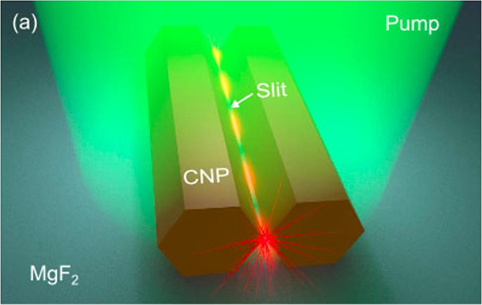
Figure 1.Schematic illustration of a CNP-based nanolaser with rod diameter of 170 nm and slit width of 1 nm (reproduced from Ref.
Since the CNP waveguide mode is not very different from those of ordinary optical waveguides except for the nm feature, one would expect that light can be efficiently coupled into the waveguide mode with appropriate impedance matching. Tong and coworkers show in the recent article6 that by using a tapering optical fiber to transfer light into the CNP along its length (Fig. 2), the transfer efficiency of visible light can be as high as 95% with
Sign up for Advanced Photonics TOC. Get the latest issue of Advanced Photonics delivered right to you!Sign up now
![]()
Figure 2.Schematic of coupling of light from a tapered optical fiber into a CNP waveguide in a distributive way along the length of the waveguide (reproduced from Ref.
The calculation in Ref. 6 is based on the assumption that wave propagation in the CNP waveguide is linear. This limits the results to cases where energy or power propagating through the waveguide is not very high. If
The CNP waveguide is potentially applicable to scanning nanoscopy, but like all near-field microscopic techniques, its resolution depends on how far a sample can be placed away from the end surface of the CNP. The nm-peak of the emitted light from a CNP is expected to spread out in free space very rapidly; a 1-nm emission spot will expand to
Field confinement in space is analogous to pulse compression in time. Confinement below a wavelength is equivalent to pulse compression to less than a cycle. If partial nm confinement is possible, one may wonder whether, similarly, partial compression of a pulse to a temporal structure much shorter than a period, say, an attosecond spike on a fs pulse, is also achievable. This is probably a far-fetched idea not physically realizable.
Yuen-Ron Shen is a professor of the Graduate School at UC Berkeley. His research is in the broad area of interaction of light with matter comprising condensed matter physics, molecular physics, nonlinear optics, laser spectroscopy, and surface sciences. He obtained his PhD from Harvard University in 1963 and joined UC Berkeley as faculty in 1964. He served as principal investigator at Lawrence Berkeley National Laboratory from 1967 to 2007. He is a member of the American Academy of Arts and Sciences, the National Academy of Sciences, the Chinese Academy of Sciences, and Academia Sinica.
References
[1] D. W. Pohl. Optical near field scanning microscope(1984).


Set citation alerts for the article
Please enter your email address

© Copyright 2018-2021 | Chinese Laser Press. All Rights Reserved 沪ICP备15018463号-20