• Acta Photonica Sinica
  • Vol. 52, Issue 8, 0823003 (2023)
Ruixue LIU, Zheng ZHANG, Jian WU, Zhen YANG, Wei WANG, Tengxiu WEI, and Rongping WANG*
Author Affiliations
  • Laboratory of Infrared Material and Devices,Advanced Technology Research Institute,Ningbo University,Ningbo 315211,China
  • show less
    DOI: 10.3788/gzxb20235208.0823003 Cite this Article
    Ruixue LIU, Zheng ZHANG, Jian WU, Zhen YANG, Wei WANG, Tengxiu WEI, Rongping WANG. Erbium-doped Ga2O3 Waveguide for Optical Amplification[J]. Acta Photonica Sinica, 2023, 52(8): 0823003 Copy Citation Text show less

    Abstract

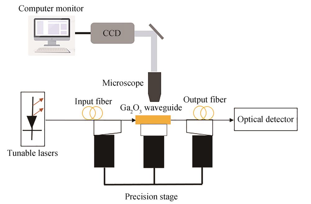
    The commercial success of Erbium-doped Optical Fiber Amplifier (EDFA) is stimulating the development of Erbium-doped Waveguide Amplifier (EDWA) which is expected to play a key component in the long-distance optical communication system in the future due to its compacted volume and low power consuming. Er ions can emit strong light at 1.55 μm that coincides with the optical communication wavelength. Therefore, when Er3+ ions are doped in a compacted waveguide structure, these ions can be excited by pump light to emit near 1.55 μm and thus amplify the signal light. Numerous studies have shown that, the fluorescence performance of Er3+ is closely related to the factors like matrix material, doping method, preparation and annealing conditions. Especially, many available Er3+-doped matrix materials have been studied so far, some of which show good properties in achieving compacted and high-gain waveguides. Among them, Er doped Al2O3 waveguide has been demonstrated to have excellent performance in optical amplification. Ga is located at the same group of Al, and thus gallium oxide (Ga2O3) has similar physical and chemical properties of Al2O3. Meanwhile, Ga2O3 has many unique advantages, such as high Er3+ doping, broad half width of full maximum in photoluminescent peak at 1.55 μm and high refractive index. Therefore, Ga2O3 has the potential to be used as a host material to fabricate planar optical waveguide device for optical amplification, however, there are no such reports in the literature. In this paper, the fabrication and properties of the erbium-doped gallium oxide films are reported. The films are characterized by Scanning Electron Microscopy (SEM) and X-ray Diffraction (XRD). The effect of the Er-doping concentration, thermal annealing temperature and film thickness on the photoluminescence properties are studied. The results show that the films are amorphous even at an annealing temperature up to 600 ℃. The maximum photoluminescence intensity appears in the film prepared at 40 W erbium oxide sputtering power and 600 ℃ annealing temperature. After optimizing the film performance, we start structural design of the Ga2O3 waveguide. Considering the fact that the fluorine-based gas reacts with Ga2O3 to form volatile gas and non-volatile GaFx is easily adhered to the surface of the film that is difficult to be removed, fluorine-based plasma is not effective in etching Ga2O3. On the other hand, direct etching of the materials containing metallic rare earth element usually leads to the aggregation of the residual metallic Er due to the different etching rate between the host materials and Er. Both could result in a very rough etched surface in the waveguide. In order to solve this problem, two kinds of waveguide structures, e.g., erbium-doped Ga2O3 film filled into SiO2 channel and erbium-doped Ga2O3 film coated on the top of the SiO2 ridge waveguide, are designed to avoid the issues caused by direct etching of Er-doped Ga2O3 film. The light field distribution in these two types of waveguides are simulated in order to maximize the interaction between the light and the effective Er-doped area. Then the waveguides are prepared based on the structural parameters from the simulation, the silicon wafer with a 2 μm thick thermally oxidized layer is used to prepare SiO2 channel and ridge structures via lithographing and etching by Ar/CHF3 etching gas, and then Er-doped Ga2O3 film with a thickness of about 400~500 nm is deposited on these structures to get the final waveguide structure. The minimum propagation loss at 1 310 nm is 1.26 dB/cm. In the future, it is expected to optimize the processing conditions of thin films and waveguides and reduce the optical loss, which could provide the possibility for the preparation of erbium-doped waveguide amplifier with better performance.
    Ruixue LIU, Zheng ZHANG, Jian WU, Zhen YANG, Wei WANG, Tengxiu WEI, Rongping WANG. Erbium-doped Ga2O3 Waveguide for Optical Amplification[J]. Acta Photonica Sinica, 2023, 52(8): 0823003
    Download Citation