
Zhe Zhuang, Daisuke Iida, Kazuhiro Ohkawa, "Ultrasmall and ultradense InGaN-based RGB monochromatic micro-light-emitting diode arrays by pixilation of conductive p-GaN," Photonics Res. 9, 2429 (2021)
- Photonics Research
- Vol. 9, Issue 12, 2429 (2021)
Abstract
1. INTRODUCTION
Owing to their high efficiency, brightness, and stability, InGaN-based micro-light-emitting diodes (μLEDs) have been considered as core devices in next-generation displays for a wide variety of applications, e.g., wall displays/televisions, smartphones/watches, head-up displays, pico-projectors, and augmented-reality (AR) glasses [1–3]. The full-color μLED displays require integration of red, green, and blue (RGB) μLEDs (R: AlGaInP; G and B: InGaN) on the same panel by pick-and-place technologies. However, the different material systems might cause mismatched far-field radiation patterns for RGB μLEDs [4], leading to a negative visual experience.
Most importantly, the high surface recombination velocities and long carrier diffusion lengths for AlGaInP materials will drastically reduce the efficiency of red μLEDs when the μLED dimensions shrink below 25 μm [5–7]. As a result, InGaN is gathering growing interest as an alternative red μLED candidate.
Despite the good performance of green/blue μLEDs, InGaN-based red μLEDs require an increase in the In-content in InGaN quantum wells (QWs), which will cause significant reduction in efficiency due to the degraded crystal quality of high-In-content InGaN QWs [8]. To solve this problem, special substrates/templates were proposed for high-In-content InGaN growth, such as InGaNOS [9],
Sign up for Photonics Research TOC. Get the latest issue of Photonics Research delivered right to you!Sign up now
Besides, ultrasmall (
To avoid the drawbacks of mesa etching, the research group from Samsung Ltd. proposed a new pixilation strategy [21] in which it tailored ion implantation to fabricate pixelated InGaN μLEDs and demonstrated high (2000−5000) pixels per inch (PPI) μLED displays with monolithically integrated thin-film transistor pixel circuits. However, this tailored ion implantation should be precisely controlled, which complicates the fabrication process. A simple strategy is more favorable for this kind of pixilation process.
In this work, we describe 5 μm squircle InGaN-based RGB monochromatic μLEDs with an interpitch of 4 μm using
2. EXPERIMENTAL DETAILS
InGaN-based red LED epitaxial wafers were grown on
The schematic of fabrication processes via pixilation of the conductive p-GaN is shown in Fig. 1. The indium tin oxide (ITO) micro-pillars arrays (
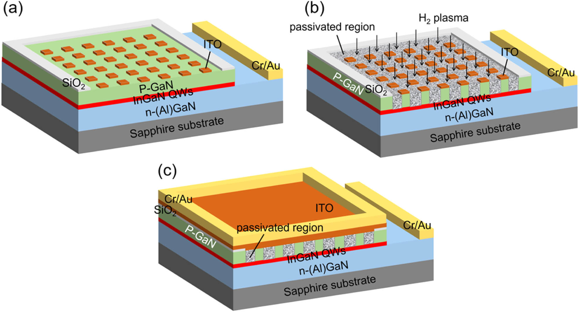
Figure 1.Schematics of fabrication processes for InGaN-based RGB monochromatic μLEDs by pixilation of conductive p-GaN.
The InGaN-based RGB monochromatic μLEDs were characterized at a probe station using a semiconductor parameter analyzer at room temperature. The EL properties were measured by the on-wafer testing, which had a similar configuration to the previous work [29]. A CCD camera installed on the microscope at the probe station was used to capture the emission patterns of these RGB monochromatic μLEDs.
3. RESULTS AND DISCUSSION
We first examined the contacts between the passivated p-GaN and the ITO layer. The absolute current of the blue LED with the passivated p-GaN was measured under the applied voltage from
![]()
Figure 2.
The absolute current-voltage (
In addition, we noticed that the currents at 4 V for the RGB μLEDs were above
At the reverse voltage, the reverse current remained constant for green/blue monochromatic μLEDs. However, the reverse current for the red μLEDs increased after the reverse voltage was above
Figure 3(a) shows the EL spectra of the RGB monochromatic μLEDs at 11.5 to
![]()
Figure 3.(a) EL spectra. (b) FWHM of RGB monochromatic μLEDs at 11.5 to
The peak wavelengths of the RGB monochromatic μLEDs exhibited the blueshift as the current density increased in Fig. 3(a). However, the blueshift values from 11.5 to
We also extracted and compared the FWHMs of the RGB monochromatic μLEDs, as shown in Fig. 3(b). The FWHMs at
The on-wafer LOP density can be used to evaluate the brightness of μLEDs. Figure 4 shows that the calculated on-wafer LOP density of green μLEDs is slightly lower than that of blue μLEDs. However, the LOP density of the red μLEDs is almost one order of magnitude lower than that of the green/blue μLEDs at the same current density. Besides, the LOP density of the red μLEDs decreased faster as the current density decreased when compared with the green/blue μLEDs. The phenomenon can be explained by the dominant Shockley–Read–Hall (SRH) recombination at lower current densities. Compared with green/blue μLEDs, red μLEDs have more defects in the active region. These defects serve as the SRH recombination centers and suppress the radiative recombination, especially at the lower current densities [34]. Therefore, less percent of carriers contribute to the light output and result in further reduction of the LOP density for red μLEDs as the current density decreases.
![]()
Figure 4.On-wafer LOP density of RGB monochromatic μLEDs at different current densities.
Because of the lower LOP density, the red μLEDs require to be operated at a higher current density to achieve a similar brightness to that of the green/blue μLEDs. Generally, AR head-mounted displays need to achieve very high brightness (
We also compared the performance of the red μLEDs with other works [9,11,13,35,36]. As shown in Table 1, the red μLEDs in this work realized the highest current density at the emission wavelength around 630 nm. As a result, the LOP density of the red μLEDs reaches approximately
Comparison of LOP Density for InGaN-Based Red μLEDs
| Affiliation | Peak Wavelength (nm) | Current Density ( | LOP Density ( |
|---|---|---|---|
| KAUST (this work) | 632 | 115 | 936 |
| KAUST [ | 626 | 4 | 29 |
| KAUST [ | 630 | 50 | 176 |
| UCSB [ | 632 | 10 | 40 |
| Univ. of Grenoble-Alpes [ | 630 | 0.8 | 0.4 |
| Plessey [ | 630 | 10 | — |
Figures 5(a)−5(c) show the EL emission images of RGB monochromatic μLED arrays at
![]()
Figure 5.(a)−(c) EL emission images of RGB monochromatic μLED arrays at
We also calculated the coordinates of RGB monochromatic μLEDs at 11.5 and
4. CONCLUSION AND PROSPECT
In summary, here we have demonstrated that the p-GaN was passivated after
To realize full-color displays, the research group from Samsung Ltd. utilized the pixilation of blue μLEDs by ion implantation and chose quantum dot color converters for red/green μLEDs [21]. They avoided the mass transfer process and realized the prototype of micro-displays. In the case of RGB monochromatic μLEDs, the full-color displays generally need to assemble individual RGB μLEDs side-by-side via mass transfer. But this integration method is not suitable for the proposed pixilation method in this work. Another approach is vertically stacking the monochromatic μLED arrays, which was demonstrated by Lee
Acknowledgment
Acknowledgment. The fabrication processes in this work were supported by Nanofabrication Core Labs in KAUST.
References
[1] Z. Chen, S. Yan, C. Danesh. MicroLED technologies and applications: characteristics, fabrication, progress, and challenges. J. Phys. D, 54, 123001(2021).
[2] H. S. Wasisto, J. D. Prades, J. Gülink, A. Waag. Beyond solid-state lighting: miniaturization, hybrid integration, and applications of GaN nano- and micro-LEDs. Appl. Phys. Rev., 6, 041315(2019).
[3] P. J. Parbrook, B. Corbett, J. Han, T.-Y. Seong, H. Amano. Micro-light emitting diode: from chips to applications. Laser Photon. Rev., 15, 2000133(2021).
[4] F. Gou, E.-L. Hsiang, G. Tan, P.-T. Chou, Y.-L. Li, Y.-F. Lan, S.-T. Wu. Angular color shift of micro-LED displays. Opt. Express, 27, A746-A757(2019).
[5] J.-T. Oh, S.-Y. Lee, Y.-T. Moon, J. H. Moon, S. Park, K. Y. Hong, K. Y. Song, C. Oh, J.-I. Shim, H.-H. Jeong, J.-O. Song, H. Amano, T.-Y. Seong. Light output performance of red AlGaInP-based light emitting diodes with different chip geometries and structures. Opt. Express, 26, 11194-11200(2018).
[6] M. S. Wong, J. A. Kearns, C. Lee, J. M. Smith, C. Lynsky, G. Lheureux, H. Choi, J. Kim, C. Kim, S. Nakamura, J. S. Speck, S. P. DenBaars. Improved performance of AlGaInP red micro-light-emitting diodes with sidewall treatments. Opt. Express, 28, 5787-5793(2020).
[7] S. Sinha, F. G. Tarntair, C. H. Ho, Y. R. Wu, R. H. Horng. Investigation of electrical and optical properties of AlGaInP red vertical micro-light-emitting diodes with Cu/Invar/Cu metal substrates. IEEE Trans. Electron Devices, 68, 2818-2822(2021).
[8] B. Damilano, B. Gil. Yellow-red emission from (Ga,In)N heterostructures. J. Phys. D, 48, 403001(2015).
[9] A. Dussaigne, F. Barbier, B. Damilano, S. Chenot, A. Grenier, A. M. Papon, B. Samuel, B. B. Bakir, D. Vaufrey, J. C. Pillet, A. Gasse, O. Ledoux, M. Rozhavskaya, D. Sotta. Full InGaN red light emitting diodes. J. Appl. Phys., 128, 135704(2020).
[10] T. Ozaki, M. Funato, Y. Kawakami. Red-emitting In
[11] S. S. Pasayat, C. Gupta, M. S. Wong, R. Ley, M. J. Gordon, S. P. DenBaars, S. Nakamura, S. Keller, U. K. Mishra. Demonstration of ultra-small <10 μm) 632 nm red InGaN micro-LEDs with useful on-wafer external quantum efficiency (>0.2%) for mini-displays. Appl. Phys. Express, 14, 011004(2020).
[12] K. Ohkawa, T. Watanabe, M. Sakamoto, A. Hirako, M. Deura. 740-nm emission from InGaN-based LEDs on
[13] Z. Zhuang, D. Iida, K. Ohkawa. Investigation of InGaN-based red/green micro-light-emitting diodes. Opt. Lett., 46, 1912-1915(2021).
[14] H. Yu, M. H. Memon, D. Wang, Z. Ren, H. Zhang, C. Huang, M. Tian, H. Sun, S. Long. AlGaN-based deep ultraviolet micro-LED emitting at 275 nm. Opt. Lett., 46, 3271-3274(2021).
[15] J. Yu, T. Tao, B. Liu, F. Xu, Y. Zheng, X. Wang, Y. Sang, Y. Yan, Z. Xie, S. Liang, D. Chen, P. Chen, X. Xiu, Y. Zheng, R. Zhang. Investigations of sidewall passivation technology on the optical performance for smaller size GaN-based micro-LEDs. Crystals, 11, 403(2021).
[16] S. S. Konoplev, K. A. Bulashevich, S. Y. Karpov. From large-size to micro-LEDs: scaling trends revealed by modeling. Phys. Status Solidi A, 215, 1700508(2018).
[17] P. F. Tian, J. J. D. McKendry, Z. Gong, B. Guilhabert, I. M. Watson, E. D. Gu, Z. Z. Chen, G. Y. Zhang, M. D. Dawson. Size-dependent efficiency and efficiency droop of blue InGaN micro-light emitting diodes. Appl. Phys. Lett., 101, 231110(2012).
[18] J. Kou, C.-C. Shen, H. Shao, J. Che, X. Hou, C. Chu, K. Tian, Y. Zhang, Z.-H. Zhang, H.-C. Kuo. Impact of the surface recombination on InGaN/GaN-based blue micro-light emitting diodes. Opt. Express, 27, A643-A653(2019).
[19] M. S. Wong, C. Lee, D. J. Myers, D. Hwang, J. A. Kearns, T. Li, J. S. Speck, S. Nakamura, S. P. DenBaars. Size-independent peak efficiency of III-nitride micro-light-emitting-diodes using chemical treatment and sidewall passivation. Appl. Phys. Express, 12, 097004(2019).
[20] J. M. Smith, R. Ley, M. S. Wong, Y. H. Baek, J. H. Kang, C. H. Kim, M. J. Gordon, S. Nakamura, J. S. Speck, S. P. DenBaars. Comparison of size-dependent characteristics of blue and green InGaN microLEDs down to 1 μm in diameter. Appl. Phys. Lett., 116, 071102(2020).
[21] J. Park, J. H. Choi, K. Kong, J. H. Han, J. H. Park, N. Kim, E. Lee, D. Kim, J. Kim, D. Chung, S. Jun, M. Kim, E. Yoon, J. Shin, S. Hwang. Electrically driven mid-submicrometre pixilation of InGaN micro-light-emitting diode displays for augmented-reality glasses. Nat. Photonics, 15, 449-455(2021).
[22] D. Iida, Z. Zhuang, P. Kirilenko, M. Velazquez-Rizo, M. A. Najmi, K. Ohkawa. 633-nm InGaN-based red LEDs grown on thick underlying GaN layers with reduced in-plane residual stress. Appl. Phys. Lett., 116, 162101(2020).
[23] D. Iida, K. Niwa, S. Kamiyama, K. Ohkawa. Demonstration of InGaN-based orange LEDs with hybrid multiple-quantum-wells structure. Appl. Phys. Express, 9, 111003(2016).
[24] D. Iida, S. Lu, S. Hirahara, K. Niwa, S. Kamiyama, K. Ohkawa. Enhanced light output power of InGaN-based amber LEDs by strain-compensating AlN/AlGaN barriers. J. Cryst. Growth, 448, 105-108(2016).
[25] T. Sugiyama, D. Iida, T. Yasuda, M. Iwaya, T. Takeuchi, S. Kamiyama, I. Akasaki. Extremely low-resistivity and high-carrier-concentration Si-doped Al0.05Ga0.95N. Appl. Phys. Express, 6, 121002(2013).
[26] Z. Zhuang, D. Iida, P. Kirilenko, M. Velazquez-Rizo, K. Ohkawa. Optimal ITO transparent conductive layers for InGaN-based amber/red light-emitting diodes. Opt. Express, 28, 12311-12321(2020).
[27] A. Y. Polyakov, N. B. Smirnov, A. V. Govorkov, K. H. Baik, S. J. Pearton, B. Luo, F. Ren, J. M. Zavada. Hydrogen plasma passivation effects on properties of p-GaN. J. Appl. Phys., 94, 3960-3965(2003).
[28] H. Fu, K. Fu, H. Liu, S. R. Alugubelli, X. Huang, H. Chen, J. Montes, T.-H. Yang, C. Yang, J. Zhou, F. A. Ponce, Y. Zhao. Implantation-and etching-free high voltage vertical GaN p–n diodes terminated by plasma-hydrogenated p-GaN: revealing the role of thermal annealing. Appl. Phys. Express, 12, 051015(2019).
[29] Z. Zhuang, D. Iida, M. Velazquez-Rizo, K. Ohkawa. 606-nm InGaN amber micro-light-emitting diodes with an on-wafer external quantum efficiency of 0.56%. IEEE Electron Device Letters, 42, 1029-1032(2021).
[30] T. Zhi, T. Tao, B. Liu, Z. Xie, P. Chen, R. Zhang. Reverse leakage current characteristics of GaN/InGaN multiple quantum-wells blue and green light-emitting diodes. IEEE Photon. J., 8, 1601606(2016).
[31] Z. Zhuang, D. Iida, K. Ohkawa. Effects of size on the electrical and optical properties of InGaN-based red light-emitting diodes. Appl. Phys. Lett., 116, 173501(2020).
[32] J. I. Hwang, R. Hashimoto, S. Saito, S. Nunoue. Development of InGaN-based red LED grown on (0001) polar surface. Appl. Phys. Express, 7, 071003(2014).
[33] S. Okamoto, N. Saito, K. Ito, B. Ma, K. Morita, D. Iida, K. Ohkawa, Y. Ishitani. Energy transport analysis in a Ga0.84In0.16N/GaN heterostructure using microscopic Raman images employing simultaneous coaxial irradiation of two lasers. Appl. Phys. Lett., 116, 142107(2020).
[34] D. S. Meyaard, Q. Shan, J. Cho, E. F. Schubert, S.-H. Han, M.-H. Kim, C. Sone, S. J. Oh, J. K. Kim. Temperature dependent efficiency droop in GaInN light-emitting diodes with different current densities. Appl. Phys. Lett., 100, 081106(2012).
[35] Z. Zhuang, D. Iida, M. Velazquez-Rizo, K. Ohkawa. 630-nm red InGaN micro-light-emitting diodes (<20 μm × 20 μm) exceeding 1 mW/mm2 for full-color micro-displays. Photon. Res., 9, 1796-1802(2021).
[36] Y. Chen. Plessey achieves native red InGaN LEDs on silicon for full color micro LED displays.
[37] J.-H. Kang, B. Li, T. Zhao, M. A. Johar, C.-C. Lin, Y.-H. Fang, W.-H. Kuo, K.-L. Liang, S. Hu, S.-W. Ryu, J. Han. RGB arrays for micro-light-emitting diode applications using nanoporous GaN embedded with quantum dots. ACS Appl. Mater. Interfaces, 12, 30890-30895(2020).
[38] S.-W. H. Chen, Y.-M. Huang, K. J. Singh, Y.-C. Hsu, F.-J. Liou, J. Song, J. Choi, P.-T. Lee, C.-C. Lin, Z. Chen, J. Han, T. Wu, H.-C. Kuo. Full-color micro-LED display with high color stability using semipolar (20-21) InGaN LEDs and quantum-dot photoresist. Photon. Res., 8, 630-636(2020).
[39] C.-M. Kang, D.-J. Kong, J.-P. Shim, S. Kim, S.-B. Choi, J.-Y. Lee, J.-H. Min, D.-J. Seo, S.-Y. Choi, D.-S. Lee. Fabrication of a vertically-stacked passive-matrix micro-LED array structure for a dual color display. Opt. Express, 25, 2489-2495(2017).
[40] K. Yadavalli, C.-L. Chuang, H. El-Ghoroury. Monolithic and heterogeneous integration of RGB micro-LED arrays with pixel-level optics array and CMOS image processor to enable small form-factor display applications. Proc. SPIE, 11310, 113100Z(2020).


Set citation alerts for the article
Please enter your email address

© Copyright 2018-2021 | Chinese Laser Press. All Rights Reserved 沪ICP备15018463号-20