You Sin Tan, Hao Wang, Hongtao Wang, Chengfeng Pan, Joel K. W. Yang, "High-throughput fabrication of large-scale metasurfaces using electron-beam lithography with SU-8 gratings for multilevel security printing," Photonics Res. 11, B103 (2023)
Copy Citation Text
The field of metasurface research has rapidly developed in the past decade. Electron-beam lithography (EBL) is an excellent tool used for rapid prototyping of metasurfaces. However, Gaussian-beam EBL generally struggles with low throughput. In conjunction with the recent rise of interest in metasurfaces made of low-index dielectric materials, we propose in this study the use of a relatively unexplored chemically amplified resist, SU-8 with EBL, as a method for rapid prototyping of low-index metasurfaces. We demonstrate the use of SU-8 grating on silicon for cost-efficient fabrication of an all-dielectric multilevel security print for anti-counterfeiting purposes, which encrypt different optical information with different light illumination conditions, namely, bright-field reflection, dark-field reflection, and cross-polarized reflection. The large-scale print () could be exposed in a relatively short time () due to the ultrahigh sensitivity of the resist, while the feature size of was maintained, demonstrating that SU-8 EBL resist serves as a good candidate for rapid prototyping of metasurface designs. Our results could find applications in the general area of increasing EBL patterning speed for a variety of other devices and structures.
1. INTRODUCTION
The study in metasurface for the manipulation of electromagnetic waves has surged rapidly in the past decades, due to its ability to control the local properties of the effective permittivity and permeability of materials [1,2]. To date, various devices and applications have been developed from metasurface-based flat optics, such as metalenses [3–7], color filters [8–14], orbital angular momentum (OAM) generators [15–17], holography [8,18–21], and beam-steering devices [22,23].
Typically, the metasurface is prototyped and fabricated using a direct writing lithography (DWL) system, such as electron-beam lithography (EBL) and focus ion beam (FIB) lithography [24–27]. These methods suffer from low throughput [28–30] and are not suitable for large-scale manufacturing. Optical photolithography [31–34] and nanoimprint lithography [35–40] have been proposed and demonstrated as potential solutions to increase the throughput. However, the demand for a predesigned mold/mask imposes a strict design requirement on the simulated performance of the device and has very low tolerance to the design error. Electron-beam lithography tools with high throughput include shaped-beam systems [28,41] that are very expensive and often beyond the reach of academic institutions and startups. Therefore, it is crucial to have a low-cost but high-speed process that allows large scale metasurface fabrication with nanoscale feature size using DWL. Such a process could reduce the prototyping time and allow quick transition to mask/mold-based methods for mass production.
One promising option to increase the throughput for DWL is to make use of high-sensitivity resists such as chemically amplified resists [42–44]. Among them, SU-8 is one of the most common available options for EBL. SU-8 resist is better known as a negative-tone photoresist [30,45,46]. However, it can also be used as a negative-tone electron-beam resist with several advantages over the more widely used negative-tone electron-beam resist, hydrogen silsesquioxane (HSQ). First, SU-8 is a chemically amplified resist that has a much higher sensitivity compared to the usual electron-beam resist [44,47]. From the reported studies, the onset dose of SU-8 to HSQ could be up to 1000 times smaller [43,44,48,49], which implies a reduction in exposure time of at least 1000 times for a given pattern. Second, crosslinked SU-8 is an optically transparent epoxy that can be removed easily with solvents such as acetone or n-methyl-2-pyrrolidone (NMP), or simple physical oxygen plasma treatment [50], unlike HSQ, which requires hydrofluoric acid (HF). For many applications, these properties allow substrates to be reused in the process of optimizing exposure parameters.
In the past, the study on the use of SU-8 as an electron-beam resist is less common, as it suffers from low resolution and high proximity effects [44]. Thus, the use of electron-beam patterned SU-8 is limited to gray-scale lithography [30,51] and microfluidic applications [45,50]. However, there is a recent surge of interest in the study on metasurfaces with near-wavelength periodicity, which contain lots of intriguing phenomena not observable in the subwavelength regime and diffraction regime [52,53]. Moreover, metasurfaces with near-wavelength periods will likely face smaller obstacles for transition into industrial-scale mass production, as they have much greater tolerance to fabrication imperfections than those requiring smaller feature sizes. Hence, SU-8 resist is very compatible with the development of metasurfaces with near-wavelength period and could potentially serve as an alternative process for rapid prototyping and fabrication of large-scale metasurfaces with relatively large pitch () and small fill factor () [43,44,47]. The large-scale metasurfaces in this regime are suitable for devices and applications in visible light manipulation and structural color design. Coincidently, there has also been a great interest in recent years to generate bright vivid colors from low-refractive-index polymeric materials such as biodegradable polymers and plastics, which have gained extensive attention due to their environmentally friendly characteristics, vast availability, and low cost [54–57]. Therefore, it is intriguing to realize structural coloration with unique spectral properties by applying these cost-effective materials.
In this work, we propose and demonstrate a new strategy to make use of electron-beam patterned shallow SU-8 polymer one-dimensional (1D) grating structures on an ordinary silicon substrate for high-throughput fabrication of large-scale metasurfaces used in the visible light regime. By using SU-8 grating structures with near-wavelength period, we show that one could encrypt vivid color information under dark-field illumination by making use of the diffraction and Bragg interference effect [58,59] without plasmon resonance and Mie resonance. In addition, by using the symmetry-protected color-independent properties of the grating orientation under dark-field illumination, we further introduced a mechanism for encrypting extra information in cross-polarization reflection. Under cross-polarization reflection, due to the birefringence properties [60–62] of the gratings, the gratings orientated at will appear dark, while the grating oriented at will be bright. Taking use of these different grating orientations, we demonstrate an all-dielectric multilevel security color print that encrypts two different optical information in dark-field illumination and cross-polarization reflection with very low cross talk. The proposed devices have potential applications for security-printing, information encryption, and optical data storage. Furthermore, benefitting from the simple and high-throughput fabrication process, the SU-8 polymer-on-silicon design enables a cost-effective fabrication process, and the substrate can be effectively recycled by dissolving the resist, promoting the development of the green manufacturing.
2. EXPERIMENT METHODS
A. Electron-Beam Lithography
The diluted SU-8 2000 resist with a solid concentration of 18% (mass fraction) was spin-coated on a silicon substrate at 3000 revolutions per minute (r/min) for 1 min to produce a film with thickness of . Prebaking of the sample was performed on a hotplate at 100°C for 5 min. The electron-beam exposure was performed using Raith eLine Plus at 30 kV accelerating voltage and beam current with exposure dose of μ. No post-baking was performed after the exposure to reduce residual layer formation and to avoid thermally induced crosslinking effects, which may affect the dimension of the patterned structures [43,47,63,64]. The sample was developed at room temperature by dipping in propylene glycol monomethyl ether acetate (PGMEA) solution for 1 min followed by dipping in isopropyl alcohol (IPA) solution for 10 s and rinsing in running deionized (DI) water for 30 s. Finally, the sample was blow-dried with a steady stream of nitrogen () gas. The patterned polymer resist can be easily removed by oxygen plasma treatment or chemical immersion in acetone or NMP, hence recycling the substrate.
B. Optical Imaging and Characterization
The optical image was taken using an upright compound microscope (Nikon Eclipse LV100ND, Nikon Instruments Inc.) with Nikon LV-HL50W halogen lamp as light source. A objective was used for all the images taken. Unless otherwise stated, all the images in dark-field mode and cross-polarization reflection mode were taken with 200 ms exposure time and 1000 ms exposure time, respectively. Under cross-polarization reflection mode, a linearly -polarized light was used as incident light, and a -polarizer was employed before the detector to collect light only polarized in the direction.
The spectral characterization of the samples was performed using the 508 PV microscope spectrometer (CRAIC Technologies) with controlling software Lambdafire. The bright-field reflection spectra and cross-polarized reflection spectra were measured by first taking the reference spectrum of a clean aluminum surface in co-polarization mode. The spectra were then measured in cross-polarization and normalized by the reference spectrum. The dark-field spectra were measured at fluorescence mode using the dark background as the reference.
C. SEM Imaging
A JEOL JSM 7600F scanning electron microscope (SEM) at 5 kV accelerating voltage and a Raith eLine Plus at 10 kV were employed to take the SEM images.
3. RESULTS
A. Concept Demonstration
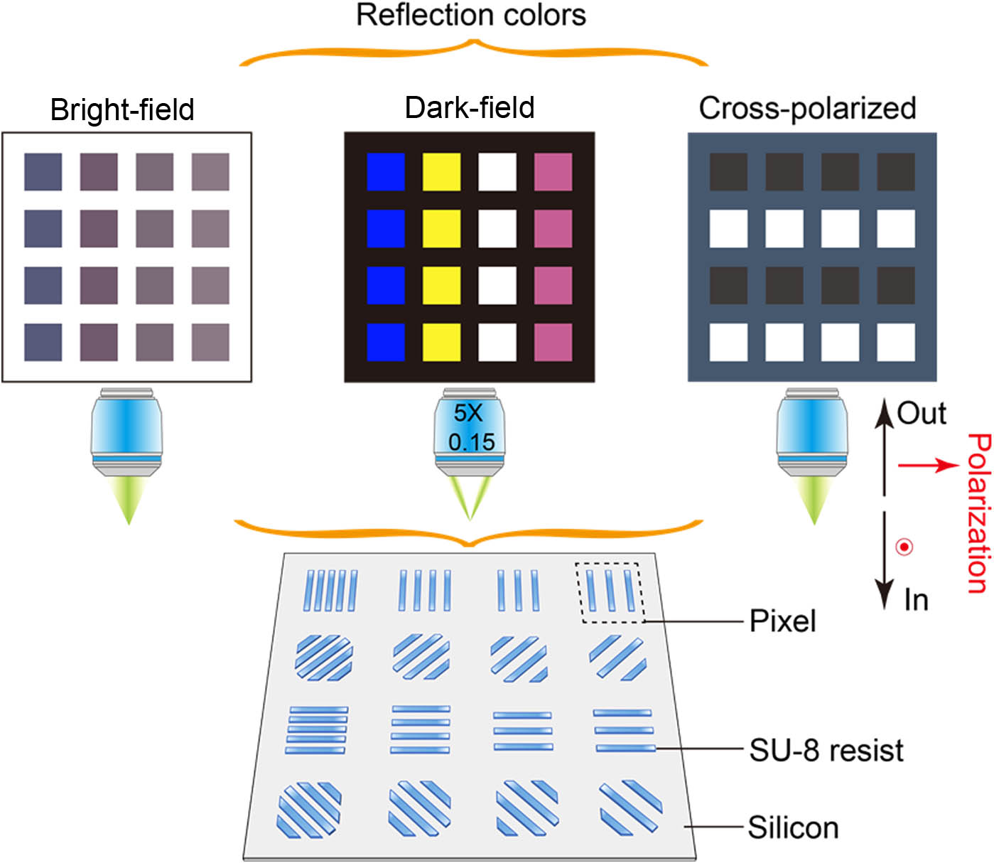
Figure 1 illustrates the concept of the proposed security print based on different light illumination methods with SU-8 gratings on silicon. Under bright-field reflection, different densities/periods of the structures will give grayscale-like color with faint hue difference, while under dark-field illumination, with different diffraction conditions, the grating structures will exhibit different colors based on the periodicity or pitch of the gratings. In addition, by making use of intrinsic circular symmetry in dark-field illumination, the grating orientation can be varied between vertical/horizontal orientation and orientation to encrypt a binary image under the cross-polarized reflection mode (-polarized incidence and -polarized reflection), without affecting the images observed under bright-field and dark-field illumination. Hence, by varying the periodicities and orientations of the gratings, one can encrypt multiple color information in a single print with minimal cross talk, which could be useful for security print and optical storage devices.
Figure 1.Schematic of the proposed SU-8 grating structures for multilevel optical security print based on different light illumination conditions, namely bright-field reflection, dark-field reflection, and cross-polarized reflection.
B. Effect of Periodicity and Exposure Dose on Bright-Field and Dark-Field Colors
We first studied the effect of grating gap and grating width on the produced colors under bright-field and dark-field illumination. Figures 2(a) and 2(b) show the micrographs of a color palette at bright-field and dark-field reflection mode for gap varying from 500 to 800 nm and width varying from 150 to 750 nm. The colors in bright-field mode are largely dependent on the grating width of the structures rather than the gap, which could be attributed to the different heights of the patterned gratings caused by dosage blurring during the exposure. The height of the grating increases with the grating width, and the change of height varies the Fabry–Perot resonances, therefore producing different colors, while the dark-field color has less dependence on the thickness of the grating structures but depends mostly on the periodicity (width + gap, along diagonal direction from bottom left corner to top right corner). This effect could be attributed to the dominant diffraction effect of the gratings. The observation of vivid dark-field color with only polymer grating on silicon has not been reported before and could be potentially useful for additional information encryption. Then, the effect of exposure dose on the produced colors under bright-field and dark-field illumination was investigated. Figures 2(c) and 2(d) show the corresponding color palette with grating period varying from 800 to 2000 nm and grating width fixed at 300 nm. The dosage was varied from 1 to μ, and the thickness of the grating structures was almost linearly increased from to . The results further confirm and strengthen our analysis that the bright-field color is more dependent on the thickness, while the dark-field color is significantly related with periodicity.
Figure 2.Bright-field and dark-field colors. (a) Bright-field and (b) dark-field reflection micrographs for gratings with gap varying from 500 to 800 nm and width varying from 150 to 750 nm. (c) Bright-field and (d) dark-field reflection micrographs for gratings with period varying from 800 to 2000 nm and grating width fixed at 300 nm. The dose factor is varying from 1 to 3.5 with base dose of μ. (e) Measured dark-field scattering spectra. (f) Corresponding color coordinates in the CIE1931 color space. (g) Illustration of maximum diffracted angle for wave diffracted to the opposite condenser. (h) Illustration of minimum diffracted angle for wave diffracted to the same condenser.
Figure 2(e) shows the measured dark-field scattering spectra for gratings with period varying from 800 to 2000 nm with grating width of 300 nm at dose of μ, and their corresponding positions in CIE1931 color space are plotted in Fig. 2(f). The large color gamut realized with the dark-field scattering spectra indicates the capabilities of SU-8 grating structures to produce vivid colors with high saturation and all hues in the visible regime.
The mechanism of dark-field scattering spectra could be explained as follows.
1. Bragg Resonance Condition for Light Coupling to Grating
By using effective medium theory [65–68], the electromagnetic (EM) waves inside the periodic grating region could be represented as Floquet–Bloch mode traveling between the top and bottom interface in a homogeneous thin film medium with effective index of : where DC is the duty cycle of the grating, is the refractive index of SU-8, and is the refractive index of air.
Substituting the expression of into Bragg’s equation, we obtain where is the incident light angle, which is equivalent to 8.6° for the objective with numerical aperture of 0.15, is the free space wavelength, and is the period of the grating.
Rearranging the equation, we can obtain
The plot of the function is depicted as the red line in Fig. 2(e), which represents the first Bragg condition for the coupling of light to grating structures used in experiment. Different wavelengths of light will be coupled to in-plane Bragg-resonance condition of grating with different periods.
2. Diffracted Condition Based on the Geometry of Objective Lens
From the anomalies/valley in the scattered spectra in Fig. 2(e), one could determine the maximum incident angle of light based on the diffraction equation In Fig. 2(e), the anomaly is observed at wavelength 676 nm for grating period of 1888 nm. Substituting the value in the diffraction equation, we obtain the maximum incident angle to be
Hence, for the microscope and objective lens used in our experiment, the light is illuminated toward specimens in a form of ring with angle ranging from 8.6° to 12° in the dark-field configuration. Different microscopes and objective lens may slightly change the range of incident angle due to the specific condenser used for dark-field illumination, which hence may cause a faint change in the observed colors and corresponding measured spectra.
Knowing the incident angle, one can further identify two diffraction effects occurring in the dark-field configuration, namely, maximum diffraction angle for light beams diffracted to the opposite condenser and minimum diffraction angle for light beams diffracted back to the incident condenser, which are depicted in Figs. 2(g) and 2(h). By fitting the diffraction conditions for two diffraction effects, one could identify the lower boundary and upper boundary of the diffraction spectra, which are represented by the white lines in the plot in Fig. 2(e). Hence, the colors of dark-field scattering of the grating structures are mainly governed by the boundaries set by the diffraction condition and Bragg coupling condition of the grating. The only collected light by the objective lens is that lying within the boundaries.
D. Cross-Polarized Reflection
With SU-8 gratings on silicon, we demonstrate the effect of “optical coloring” in the dark-field illumination. However, the dark-field illumination only encrypts the information on the colors of the structures. To design a multilevel security print, an additional degree of freedom is needed. By carefully studying the mechanism of the dark-field illumination, we notice that there is an intrinsic circular symmetry property in dark-field illumination as the light arrives at the sample in a circular ring format. Hence the grating orientation has little effect on the dark-field color due to the circular symmetry. The effect of invariant dark-field colors observed with two different grating orientations at 0° and 45° [Figs. 3(a) and 3(b)] is shown in Figs. 3(c) and 3(d). This indicates the possibility of storing additional optical information with grating orientation. Based on that, we further realized additional optical information encryption with cross-polarized reflection.
Figure 3.Cross-polarized reflection. SEM images of the grating orientations of (a) 0° and (b) 45°. (c), (d) and (e), (f) Corresponding optical micrographs under dark-field illumination and cross-polarized reflection. (g) and (h) Schematics of polarization change upon reflection from different grating orientations.
Figures 3(e) and 3(f) show the effect of different cross-polarized reflection colors observed with two different grating orientations at 0° and 45°. The gratings with 0° orientation appear dark, and gratings with 45° orientation appear bright, which could be explained with the schematics in Figs. 3(g) and 3(h) considering the polarization rotation of light upon reflection from the gratings. Here, we use Jones matrix notation to analyze the cross-polarized reflection. For a given grating structure, the reflection coefficient from the grating could be written as , where and are the reflection coefficients from transverse-electric (TE) and transverse-magnetic (TM) waves, respectively. When the grating is rotated in the propagation axis, namely, the axis, the change in reflection coefficient could be represented as , where is the rotation matrix. When the incident -polarized light is irradiated onto a rotated grating structure, the reflected light could be represented as Expanding the equation, we obtained Hence, the cross-polarized reflection is given by When the incident polarization of light is parallel to grating direction, the reflected light will have the same polarization state as the incident light, therefore it will be blocked by the cross-analyzer, and hence it will appear dark. However, when the grating is rotated, the birefringence effect is introduced for incident light beam, as the reflected beam now contains an electric field in both the parallel (TM) component and the perpendicular (TE) component to the grating wave vector direction. The surface differentiates between the TM and TE light and causes a change by introducing different time delays in the reflected components. As a result, the reflected light will become elliptically polarized, therefore it could pass through the cross-analyzer, and hence it appears bright. The intensity of cross-polarized light would be the highest when the angle of rotation is equal to 45°. This result illustrates the possibility to encrypt a binary information in the cross-polarized reflection illumination without affecting the colors observed in dark-field and bright-field illumination.
E. Demonstration of Multilevel Security Print
To employ the different responses of the proposed SU-8 grating structures on silicon under different illumination conditions, a large-scale multilevel security print () for anti-counterfeiting application was designed using grating width of 300 nm with varying period from 800 to 2000 nm. We encode the color information viewable only under dark-field illumination while simultaneously encrypting a binary image under cross-polarized illumination through different grating orientations, so the two kinds of optical information can be stored with ultralow cross talk. Due to the ultrahigh sensitivity of SU-8, the overall time taken for the exposure of the print is only about 11 min, while it takes more than 10 h for HSQ, demonstrating the possibility of high-throughput fabrication of metasurfaces using EBL with our methods. Indeed, the contrast in electron-beam writing time could be estimated theoretically by the following formula [69]: where is the electron-beam dwelling time, is the required dose, is the exposed area, and is the beam current. Equation (10) shows the relationship between the dwelling time and the clearance dose of the resist. If the beam current and the designed patterning area stay constant, then the total dwelling time will always vary linearly with the clearance dose of the resist (SU-8, μ [70]; HSQ, μ [49]). Hence, we could estimate the dwelling time as a linear function of the electron-beam dose.
A print with two different grating orientations was first fabricated for the demonstration, namely, 45° and 90°. Figure 4(a) shows the gray-scale image of butterfly print based on the density of the grating structures under bright-field illumination. Smaller periods give rise to darker color, while larger periods show lighter color. Figure 4(b) shows the “optical coloring” effect on the butterfly print with dark-field scattering and the SEM image of part of the fabricated grating structures. Furthermore, a binary image of a QR code can be observed within the same sample when the grating orientation is at 45° and examined with cross polarization, as shown in Fig. 4(d). It can be seen clearly from Fig. 4(b) that the cross talk effect is not negligible in dark-field reflection, which will affect the performance of the design and reduce the security level.
Figure 4.Multilevel security print. (a) Bright-field micrograph of grayscale image caused by different density of structures. Dark-field micrographs (top) of the image with bright and vivid colors and part of the corresponding SEM images (bottom) with (b) non-randomization and (c) randomization of grating orientations. (d) Bright-field micrograph of cross-polarized reflection of the image with the hidden information encrypted by the orientations of the gratings. (e) Bright-field micrograph of grayscale image caused by different density of structures. The “SUTD” word was exposed with dose of μ, causing it to be taller, while the rest were exposed with dose of μ. (f) Dark-field micrograph of the image with bright and vivid colors caused by diffraction effect. The “SUTD” word appears to be less obvious in the dark-field image. (g) Hidden information in bright-field cross-polarized reflection.
To solve the issue, we proceeded to study the effect of randomization of grating orientation for the print. Particularly, for gratings with 90° orientation, we introduce a randomization function such that the grating orientation will be randomly distributed as either 0° or 90°; and for gratings with 45° orientation, the same concept was applied such that the grating orientation will be randomly distributed with 45° or , as depicted in Fig. 4(c). The cross talk effect is significantly suppressed in the dark-field image, improving the performance of the security print. This cross talk suppression effect is attributed to the breaking of the geometry continuity of the structures, as the dark-field color is independent of the grating orientation. Based on the same reason, the dark-field image remains almost the same when observed with unpolarized or polarized light.
In addition, except the periodicity and orientation properties applied above, it is possible to encrypt extra information based on height of the grating structures with the result in Fig. 2. Figures 4(e)–4(g) show the effect of a simple addition of dose information on the butterfly print. In the design, we encoded an extra “SUTD” logo watermark into the print that was exposed to a dose factor of 2 during the patterning process, while the rest were exposed with dose factor of 1 with the base dose of μ. Although some cross talk could still be observed between different illumination and inspection conditions, one could easily retrieve three different types of optical information in bright-field, dark-field, and cross-polarized reflection. The cross talk could be further minimized through careful optimization of the design.
4. CONCLUSION
In summary, we have shown that it is possible to make a large-scale metasurface with high throughput by using chemically amplified resist SU-8 with EBL. This process allows significant reduction in the exposure time in fabrication of metasurface, which has potential applications in customizable mass production. We demonstrated the use of SU-8 grating on silicon for cost-efficient fabrication of a multilevel security print for anti-counterfeiting purposes that encrypt different optical information with different light illumination conditions, namely, bright-field reflection, dark-field illumination, and cross-polarized reflection. The large area print () could be exposed in a very short time () due to ultrahigh sensitivity of the resist, in which a feature size of was achieved. With post-baking for chemical amplification, it is even possible to approach the speed limit of this resist with shorter exposure time. Minimal cross talk effect between different light illumination was achieved through careful optimization of the design. The method of encrypting multilevel optical information in one print is different from the conventional ones, such as pure orthogonal polarization, multiplexing layout, and multilayer structures. Our research enriches the methods to control visual performance of optical devices and enables rapid prototyping of metasurfaces with nanoscale structures.
[24] A. Nadzeyka, S. Bauerdick, M. Kahl, H. Duan, Y. Chen, K. Bi. FIB-based sketch & peel for fast and precise patterning of large-scale nanostructures. Conference on Electron, Ion and Photon Beam Technology and Nanofabrication (EIPBN), 4(2018).
You Sin Tan, Hao Wang, Hongtao Wang, Chengfeng Pan, Joel K. W. Yang, "High-throughput fabrication of large-scale metasurfaces using electron-beam lithography with SU-8 gratings for multilevel security printing," Photonics Res. 11, B103 (2023)