
Quan You, Daigao Chen, Xi Xiao, Shaohua Yu, "10 Gb/s free space optical interconnect with broadcasting capability enabled by a silicon integrated optical phased array," Chin. Opt. Lett. 19, 120602 (2021)
- Chinese Optics Letters
- Vol. 19, Issue 12, 120602 (2021)
Abstract
1. Introduction
Optical interconnect technology has been widely used in card to card (CtC) communications and highly demanded in the servers and storage in data centers. Limited by the low speed and narrow bandwidth, traditional electrical interconnects could not be the best solution for the future service in high-capacity transmission systems. The optical wireless communications without electro-optical transformation can provide almost unlimited bandwidth connectivity to users with sample transceivers, low cost, and integrated system, which has attracted great attention in the field of free space optical interconnects[
The silicon photonic optical phased array (OPA) is also used in high-speed point to point free space communications[
2. Operation Principle
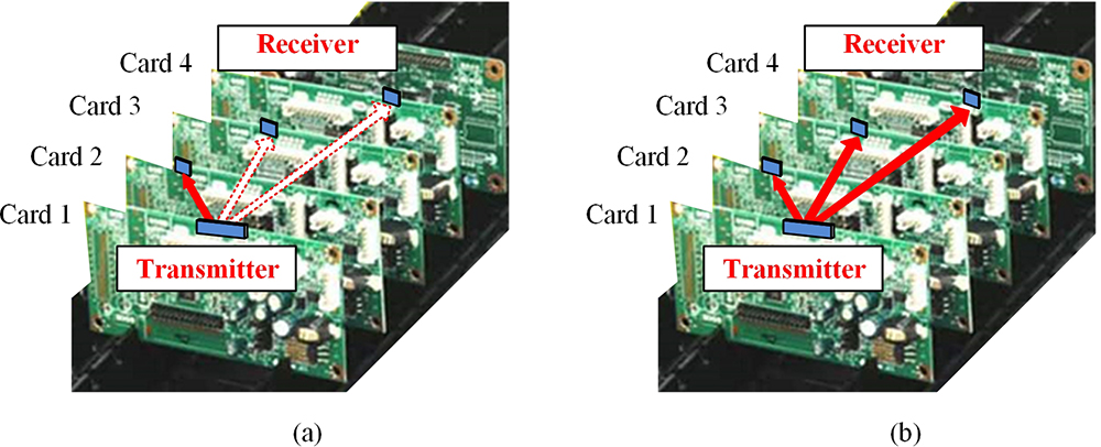
Figure 1 shows the architecture of the reconfigurable free space optical interconnect used in the field of CtC and CtMC. An optical interconnect module always includes a transmitter and a receiver integrated on a printed circuit board (PCB). The optical wavelength carried with a high data rate signal is generated by the transmitter and modulated by an OPA into optical beam forms. The optical beam is ejected into free space with scanning angles when the OPA is used for CtC transmission or separated into multiple beams when it is used for CtMC transmission. After transmitting a short distance in free space, photodiodes (PDs) located on the receiver cards are used to detect the optical signal. The multiple receivers located in different cards are served by the same transmitter and all the receivers share the same optoelectronic components like laser source and modulators.
Sign up for Chinese Optics Letters TOC. Get the latest issue of Chinese Optics Letters delivered right to you!Sign up now
![]()
Figure 1.Architecture of the proposed reconfigurable optical interconnect used in the field of (a) card to card and (b) card to multi-card.
In our reconfigurable optical broadcasting system, an eight-channel silicon integrated phased array is set at the transmitter card. The integrated silicon OPA here is fabricated on an SOI wafer with a 220 nm thick silicon layer and a 3 µm thick box layer. The width of one channel grating is 4 µm, and the channel space is 5 µm. The etching depth of the grating area is 70 nm. The gratings have a pitch of 630 nm with a duty cycle of 0.55. The device is fabricated by the commercial CMOS platform, and the whole wafer is cladded by a
![]()
Figure 2.(a) Microscope image of the proposed OPA. (b) Photo of the wire-bonded OPA on the PCB. (c) Schematic diagram of the channel grating in the proposed OPA.
We use an infrared CCD (OPHIR Photonics) at the output side of the OPA to observe near-field optical beam distribution. When the OPA is used for CtC transmission, the output beam has only one spot, as shown in Fig. 3(a). The divergence angle of the output beam is
![]()
Figure 3.Optical beam detected by an infrared CCD: (a) one spot; (b) two similar spots; (c) three similar spots; (d) five similar spots.
3. Experiments and Results
We first measured the optical power losses at different transmission distances when the OPA provided CtC service with a 0° steering angle. By using a free space optical power meter (Coherent, FieldMaxII-Top), which is set at the focal point of a lens with a focal length of 10 mm, the measured power losses are 10.1 dB, 10.6 dB, 10.9 dB, 11.1 dB, and 11.5 dB after 11 cm, 12 cm, 13 cm, 14 cm, and 15 cm transmission, as seen in Fig. 4(a). The optical power loss raised with the increasing of transmission distance; it is mainly because the beam footprints are larger after longer distance transmission, which reduces the value of optical power collected by the power meter. The end-to-end loss of the OPA device is 8 dB (including coupling loss between input fiber and OPA device) when transmission distance is 0 cm. Then, we measured the power losses versus different steering angles when the transmission distance is 15 cm. The measured optical power losses are 11.5 dB, 11.6 dB, and 11.9 dB when the steering angle is 0°, 7°, and
![]()
Figure 4.(a) Measured optical power loss versus different transmission distance with 0° steering angle. (b) Measured optical power loss versus different transmission schemes with 15 cm transmission distance.
In order to verify the directional stability of beams emitted by the OPA, we measured the centroid position of the output beam when the OPA provided CtC transmission. Here, we take the infrared CCD instead of the free space optical power meter to observe the centroid position of the output beam with 5 min spacing, and the results in 1 h measurement are shown in Table 1. The original position was measured at the fifth minute, and its coordinate was set as (0, 0). It can be seen that the centroid position of the spot was slightly moved at the room temperature of 20°C. The Gaussian beam waist at the CCD plane was
| Time (min) | 5 | 10 | 15 | 20 | 25 | 30 | 35 | 40 | 45 | 50 | 55 | 60 |
|---|---|---|---|---|---|---|---|---|---|---|---|---|
| X (mm) | 0 | 0.001 | 0.005 | 0.001 | 0 | |||||||
| Y (mm) | 0 | 0.002 | 0.001 |
Table 1. Measured Centroid Coordinates of the Output Beams with 5 min Spacing in 1 h
As shown in Fig. 5, we conduct an experiment to verify the effectiveness of the designed reconfigurable CtMC optical interconnect. First, a pseudo random binary sequence (PRBS) with length of
![]()
Figure 5.Experiment setup of the optical broadcasting system with the proposed OPA. MZM, Mach–Zehnder modulator; EDFA, erbium-doped fiber amplifier; PC, polarization controller; PD, photodiode; OPA, optical phased array.
In order to verify the steering and broadcasting functions of the optical interconnect based on the proposed experimental setup, we measured the BER performance of the signal as a function of transmission distance for the different transmission schemes, as shown in Fig. 6. The optical powers launched into the OPA device are amplified to 10 dBm by the EDFA for all three transmission schemes. Since the intensity of the optical beams is almost the same for different transmission schemes, similar BER performances are achieved. The achieved BER values are all below the 7% forward error correction (FEC) limit at the BER value of
![]()
Figure 6.BER value of the 10 Gb/s OOK signal versus transmission distance for different transmission schemes.
In our experiment, the performance of the optical broadcasting system is limited by the received optical power at the PD surface, which results in a few receiver cards getting the broadcasting signal at the same time. To solve this issue, a lower beam divergence and higher coupler efficiency OPA is needed at the transmitter side[
4. Conclusions
We have proposed and experimentally demonstrated a reconfigurable optical CtMC interconnect by using an eight-channel OPA. Based on the silicon integrated optical beam steering and broadcasting device, a 10 Gb/s optical signal is transmitted for up to three cards with
References
[1] M. A. Taubenblatt. Optical interconnects for high-performance computing. J. Lightwave Technol., 30, 448(2012).
[2] X. Zhou, H. Liu, R. Urata. Datacenter optics: requirements, technologies, and trends. Chin. Opt. Lett., 15, 120008(2017).
[3] Q. Kong, Y. Zhan, P. Wan. Hybrid OCS/OBS interconnect in intra-data-center network. Chin. Opt. Lett., 17, 080605(2019).
[4] G. Song, J. Zou, J. He. Ultra-compact silicon-arrayed waveguide grating routers for optical interconnect systems. Chin. Opt. Lett., 15, 030603(2017).
[5] Y. Li, E. Towe, M. W. Haney. Scanning the issue-special issue on optical interconnections for digital systems. Proc. IEEE, 88, 723(2000).
[6] H. Cho, P. Kapur, K. C. Saraswat. Power comparison between high-speed electrical and optical interconnects for inter-chip communication. J. Lightwave Technol., 22, 2021(2004).
[7] S. Li, Z. Wan, J. Xu, S. Zhong, Y. Wu. Wavelength-selective switch based on a high fill-factor micromirror array. Chin. Opt. Lett., 9, 090601(2011).
[8] F. Pan, L. Kong, X. Yang, Y. Ai, Y. Zhou. Dual beam deflection of liquid crystal optical phased array. Chin. Opt. Lett., 10, S20502(2012).
[9] C. J. Henderson, D. Gil-Leyva, T. D. Wilkinson. Free space adaptive optical interconnect at 1.25 Gb/s, with beam steering using a ferroelectric liquid-crystal SLM. J. Lightwave Technol., 24, 1989(2006).
[10] K. Wang, A. Nirmalathas, C. Lim, E. Skafidas, K. Alameh. High-speed reconfigurable free-space card-to-card optical interconnects. Photonics J. IEEE., 4, 1407(2012).
[11] K. Wang, A. Nirmalathas, C. Lim, E. Skafidas, K. Alameh. High-speed free-space based reconfigurable card-to-card optical interconnects with broadcast capability. Opt. Express, 21, 15395(2013).
[12] M. Aljada, K. E. Alameh, Y.-T. Lee, I.-S. Chung. High-speed (2.5Gbps) reconfigurable inter-chip optical interconnects using opto-vlsi processors. Opt. Lett., 14, 6823(2006).
[13] K. Wang, A. Nirmalathas, C. Lim, E. Wong, K. Alameh, H. Li, E. Skafidas. High-speed indoor optical wireless communication system employing a silicon integrated photonic circuit. Opt. Lett., 43, 3132(2018).
[14] H.-W. Rhee, J.-B. You, H. Yoon, K. Han, M. Kim, B. Goo Lee, S.-C. Kim, H.-H. Park. 32 Gbps data transmission with 2D beam-steering using a silicon optical phased array. IEEE Photonics Technol. Lett., 32, 843(2020).
[15] J. K. Doylend, M. J. R. Heck, J. T. Bovington, J. D. Peters, L. A. Coldren, J. E. Bowers. Free-space beam steering in two dimensions using a silicon optical phased array. Optical Fiber Communication Conference(2012).
[16] D. Kwong, A. Hosseini, J. Covey, Y. Zhang, X. Xu, H. Subbaraman, R. T. Chen. On-chip silicon optical phased array for two-dimensional beam steering. Opt. Lett., 39, 941(2014).
[17] K. Van Acoleyen, H. Rogier, R. Baets. Two-dimensional optical phased array antenna on silicon-on-insulator. Opt. Lett., 18, 13655(2010).
[18] K. Liu, Q. Wei, Y. Huang, X. Duan, Q. Wang, X. Ren, S. Cai. Integrated optoelectronic chip pair for transmitting and receiving optical signals simultaneously. Chin. Opt. Lett., 17, 041301(2019).
[19] J. He, T. Dong, Y. Xu. Review of photonic integrated optical phased arrays for space optical communication. IEEE Access, 8, 188284(2020).
[20] H.-W. Rhee, M. Kim, J.-B. You, H.-H. Park. High-speed data transmission system using silicon-based optical phased array. Proc. SPIE, 11286, 112861A(2020).
[21] M. Zadka, Y.-C. Chang, A. Mohanty, C. T. Phare, S. P. Roberts, M. Lipson. On-chip platform for a phased array with minimal beam divergence and wide field-of-view. Opt. Express, 26, 2528(2018).


Set citation alerts for the article
Please enter your email address

© Copyright 2018-2021 | Chinese Laser Press. All Rights Reserved 沪ICP备15018463号-20