
Wenbo Ren, Qingqing Liang, Jijun Feng, Haipeng Liu, Jianhua Hu, Shuo Yuan, Xincheng Xia, Wei Jiang, Qiwen Zhan, Heping Zeng. Free-space beam shaping and steering based on a silicon optical phased array[J]. Photonics Research, 2023, 11(12): 2093
- Photonics Research
- Vol. 11, Issue 12, 2093 (2023)
Abstract
1. INTRODUCTION
Laser beam shaping and steering have recently gained significant attention owing to their ability to generate unique field profiles such as vortex beams [1–3], Airy beams [4,5], and Bessel beams [6–8]. Bessel beams have the advantages such as excellent non-diffraction characteristics and parallel manipulation ability, making them suitable for various applications including multi-plane and multi-particle optical guidance and capture [9–11], microscopy for scattering reduction and field depth increase [12–14], enhancement of free-electron laser gain [15], medical coherence imaging [16], all-optical switching [17], and so forth. Additionally, Bessel beams find their application in optical manipulation of microtubule arrays for flow cytometry [18], encoding in free-space optical communication [19], optical drilling based on dynamic beam mixing [20], and preparing self-written waveguides and helical fibers through photo-polymerization [21]. Furthermore, high-order Bessel beams can be utilized for atomic guidance due to their non-diffraction properties with a minimum radius of the center around the same order as the incident wavelength [22].
Traditional beam-shaping techniques typically rely on some bulk optics elements, such as a phase mask, which can be modulated by a spatial light modulator (SLM) to generate a Bessel beam, and focused by a spherical lens in free space [18–21]. However, SLMs often have a limited resolution in phase discretization, and may not be ideal for miniaturization and high-density integration. Compact beam shaping devices, such as metasurfaces [23–26], fiber arrays [27,28], and integrated photonics chips [29–31], have been proposed as alternatives that do not require costly assembly or complex calibration processes. However, metasurfaces often require high-precision fabrication and fine calibration, and fiber arrays can be challenging for installation and adjustment due to the specific arrangement of multiple fibers. For integrated silicon photonic chips, they may generate beams with millimeter-level or longer lengths. Recently, silicon optical phased arrays (OPAs) have gained much attention due to their compatibility with complementary metal-oxide-semiconductor (CMOS) processing, making them suitable for low-cost applications. Integrated OPAs for generating quasi-Bessel beams have been presented [31], but the shaping and steering of different beam profiles have not been thoroughly investigated, despite their unprecedented flexibility in controlling electromagnetic waves. Further research in this area could unlock new possibilities for advanced beam shaping and steering applications.
In this paper, theoretical analysis of on-chip beam shaping and steering is presented, which is further experimentally verified by using a silicon OPA. The field distributions for various beam profiles are simulated first by varying phase combinations. Then, a silicon OPA with an aperture of is fabricated and tested for different beam generation. It is observed that a linear phase change can result in the generation of an ordinary Gaussian beam, with a steering angle of about . Furthermore, a quasi-Bessel beam can be shaped using a cubic phase change combination, which exhibits a hollow center with a length of about 0.77 mm and a power full width at half maximum (FWHM) of 8.5 μm. These experimental results confirm the effectiveness of the proposed approach for on-chip beam shaping and steering by a silicon OPA.
Sign up for Photonics Research TOC. Get the latest issue of Photonics Research delivered right to you!Sign up now
2. THEORETICAL BEAM SHAPING AND STEERING FOR FREE SPACE
OPA is a coherent optical emission system comprising an array of antennas that are fed with controlled phases and amplitudes to generate arbitrary radiation patterns [31–36]. The near-field electric field distribution generated by the phased array can be approximately obtained by summing the electric field components of each element () in the array as
Applying the axicon-like element phase distribution of bulk optics on the basis of amplitude, different shape of light beam can be generated in the near field, and the th-order axicon phase can be obtained by the following formula [31]:
Here, is the array factor that affects the far-field interference pattern of the beam, and is a variable initial phase. To explore the influence of phased array elements on the beam under the application of different variable phase parameters, representative variable phase parameters are selected. The variable phase parameter can be taken as , , and , respectively. For example, the corresponding phase distribution curves for and are shown in Figs. 1(a) and 1(b), respectively. When is 0 with variable phase parameter and amplitude parameter , a Gaussian beam will be generated as shown in Fig. 2(a). When is 1, 2, or 3 with the variable phase parameter of and amplitude parameter of 1, the field distributions generated by the simulated one-dimensional free space beam array are shown in Figs. 2(b)–2(d).
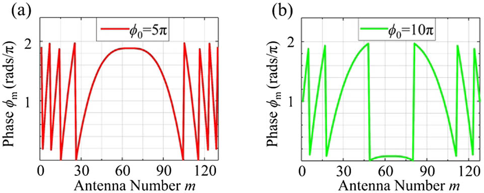
Figure 1.Element phase distribution with (a)
![]()
Figure 2.Simulated near-field distribution above the array for (a) a Gaussian beam with
From the simulated field distribution in Fig. 2(b), it can be seen that the array can generate a quasi-Bessel beam, which has been demonstrated before [31] and will not be discussed here. When , OPA can also generate a convergent beam [Fig. 2(c)]. Due to its slight similarity with the Gaussian beam, it will also be skipped for simplicity. With a cubic phase change combination of , a high-order quasi-Bessel beam can be generated, as presented in Fig. 2(d). This configuration results in the formation of a hollow-core central cavity [28]. The beam has a good propagation stability and can be used for large particle trapping, facilitating its application in optical microscopy [37] and the treatment of material surfaces [38]. For further comparison, the corresponding transverse light field distributions at the position are also shown in Figs. 2(e)-2(h), respectively. The beam profile variation from the Gaussian shape to hollow-core central cavity can be clearly seen.
![]()
Figure 3.Simulated near-field distribution above the array for the cubic phase change combination with (a)
Silicon OPAs can be programmed to steer the generated optical field. A linear change of the phase combination can realize the beam deflection, which can be expressed as
Here, is the steering coefficient, which can determine the deflection angle, and is the steering constant depending on the antenna aperture. For the presented high-order quasi-Bessel beam with a cubic phase change combination, the beam steering results can be simulated with varying . The field distribution at different deflection angle with is shown in Fig. 4. A large beam deflection angle of can be realized as shown in Figs. 4(a) and 4(d). Compared with the traditional beam-shaping technique based on bulk optics elements, OPA can achieve more flexible, accurate, and faster beam steering.
![]()
Figure 4.Simulated steering results for a quasi-Bessel beam with a cubic phase change combination and varying
3. EXPERIMENTAL RESULTS
As a proof of concept, the OPA chip was fabricated by ultraviolet (UV) lithography with a standard commercial CMOS facility. The antenna aperture size is . The OPA architecture used here is based on a splitting tree structure, as shown in Fig. 5(a). The input light couples into the waveguide via end-coupling, and is split into 128 channels by a cascaded MMI splitter. A micro-heater-based phase shifter is integrated on each channel for phase modulation, which consists of TiN with a size of and a resistance of about 1 kΩ and can achieve a -phase shifter with an 18.7 mW power consumption. Light in each channel exits into free space via the sidewall-grating-based waveguide antenna, and it interferes in the far field region. Figure 5(b) shows the packaged chip, with Fig. 5(c) for the microscope image of the fabricated chip. Figure 5(d) presents the scanning electron microscope (SEM) image of the sidewall grating waveguide antenna, which has a period of 650 nm and a duty cycle of 0.5. The sidewall grating antenna used here can help to increase the light emission length and improve the roundness of the far-field pattern. In addition, temperature is also a key factor affecting the beam shaping performance. Here, a thermo-electric cooler (TEC) was adopted in the experiment to reduce the impact of temperature.
![]()
Figure 5.(a) Schematic diagram of silicon OPA with (b) and (c) for the microscope image of the packaged device and OPA chip, respectively. (d) SEM image of the grating waveguide antenna.
The schematic diagram of the experimental device for beam shaping and control characteristics is shown in Fig. 6. A tunable laser was used as the light source at a 1550 nm wavelength, and it was connected with a polarization controller and coupled into the waveguide through a packaged lensed fiber. The output light from OPA was emitted to the free space and monitored by a charge coupled device (CCD), which was monitored by a computer. The computer then generated a required voltage combination for the control circuit, which was applied to the phase shifter above the waveguide, and the phase would change correspondingly. Through this feedback unit, a particle swarm optimization algorithm was adopted for the compensation of initial phase error caused by random non-uniformity of waveguides, which can converge more easily to an optimal solution with a fixed number of paths than the adjacent sampling principal component analysis method [39,40]. Then the specific beam profile could be generated with the desired phase combination. The CCD was mounted on a linear electric stage, to record the field distribution along the exit Z direction in the free space.
![]()
Figure 6.Schematic illustration of the experimental setup for the characterization of beam shaping and steering.
For the Gaussian beam case with , it is the normal beam steering configuration, and the recorded light intensity along the exit direction is shown in Fig. 7(a). A sidelobe suppression ratio of larger than 10 dB can be realized. The divergence angle is about 0.1°, with the cross-sectional beam profile shown in Fig. 7(b). A large steering angle of about can be achieved by a linear change of the waveguide phase, with the theoretical and experimental results shown in Figs. 7(c) and 7(d), respectively. When the input optical power is about 10 mW, the output power of the main lobe is about 15.3 μW, resulting in a total loss of about 28 dB, which is slightly high and still needs further optimization. However, the current chip can still be used for the beam-shaping and steering demonstration. Figures 8(a)–8(d) verify a quasi-Bessel beam generation with . The corresponding beam length is approximately 10.6 mm, comparable with the simulated value of 12.4 mm. The difference may come from the waveguide fabrication errors, thermal crosstalk, and free-space stray light of the device itself.
![]()
Figure 7.(a) Measured cross-sectional intensity distribution of OPA along the exit
![]()
Figure 8.(a) Measured cross-sectional intensity above the chip for a quasi-Bessel beam generation (
For the cubic phase change combination with of and , the corresponding cross-sectional intensity distribution is shown in Fig. 9, and a hollow-core beam can be generated. As can be seen from Fig. 9(a), a power FWHM of was measured along the hollow-core beam, matching the simulated value of 6.34 μm. Furthermore, a hollow core beam length of was measured, near the simulated value of 0.62 mm. The corresponding top-down views of light intensity distribution at different position above the chip are shown in Figs. 9(b)–9(d), which are near the converged region (), the hollow-core region (), and the split hollow core region () of the emitted beam, respectively. The measured results are similar to the simulated one in Fig. 3(b). The simulated light intensity distributions at the corresponding position are shown in Figs. 9(e)–9(g), respectively.
![]()
Figure 9.(a) Measured cross-sectional intensity above the chip for a high-order quasi-Bessel beam generation (
It should be noted that the theoretical results [Figs. 9(e)–9(g)] are slightly similar to the ideal higher-order Bessel beam, and thus a quasi-Bessel beam can be generated here. However, there is still some difference, which may be due to the diffraction effects originating from the chip, as well as the phase error caused by random non-uniformity of waveguides. Furthermore, the imaging quality of the infrared camera is constrained by its 20 μm resolution. The amplitude of each channel may also be slightly different, which would influence the final light field distribution, although the amplitude of each channel cannot be adjusted here. By adding a Mach–Zehnder interferometer unit to control the output light amplitude of each channel, more complex light fields can be generated. Furthermore, the simulated and measured cross-sectional intensity distributions for the emitted beam at the hollow-core region (), as well as the split hollow core region () are presented in Fig. 10. They can coincide well with each other, despite of some noisy background. Note that a larger-scale integrated OPA has been applied for the Bessel–Gaussian beam generation [41], which can be used for long-range sensing. In addition, femtosecond-laser direct writing of three-dimensional phase plates can also generate Bessel beams efficiently and quickly [42]. Here, we systematically summarized and experimentally verified the potential beam shaping and steering with silicon OPA. The presented method provides a new version for high-order quasi-Bessel beam generation, which can be expected to have broad application prospects.
![]()
Figure 10.Normalized intensity distribution of the simulated high-order quasi-Bessel beam above the chip at
4. CONCLUSION
To summarize, we have successfully demonstrated a silicon OPA for free-space beam shaping and steering. Through detailed analysis of the phase and amplitude distribution, a variety of special free-space beams can be generated, including but not limited to Gaussian and quasi-Bessel beams. Our results show that a Gaussian beam with a divergence angle of approximately 0.1° can be achieved, with a steering angle of about . Furthermore, a high-order quasi-Bessel beam can be generated with an cubic phase change combination, exhibiting a hollow length of and an FWHM of about 8.5 μm. The effectiveness of the proposed approach for on-chip beam shaping and steering can open the door to applications from optical communications to atomic guidance.
References

Set citation alerts for the article
Please enter your email address
© Copyright 2018-2021 | Chinese Laser Press. All Rights Reserved 沪ICP备15018463号-20