Abstract
Graphene and related two-dimensional materials have attracted great research interests due to prominently optical and electrical properties and flexibility in integration with versatile photonic structures. Here, we report an in-fiber photoelectric device by wrapping a few-layer graphene and bonding a pair of electrodes onto a tilted fiber Bragg grating (TFBG) for photoelectric and electric-induced thermo-optic conversions. The transmitted spectrum from this device consists of a dense comb of narrowband resonances that provides an observable window to sense the photocurrent and the electrical injection in the graphene layer. The device has a wavelength-sensitive photoresponse with responsivity up to 11.4 A/W, allowing the spectrum analysis by real-time monitoring of photocurrent evolution. Based on the thermal-optic effect of electrical injection, the graphene layer is energized to produce a global red-shift of the transmission spectrum of the TFBG, with a high sensitivity approaching 2.167×10⁴ nm/A2. The in-fiber photoelectric device, therefore as a powerful tool, could be widely available as off-the-shelf product for photodetection, spectrometer and current sensor.Introduction
Optical fiber as a milestone in optical communication, its low-loss nature makes it as a dominant player in the communication field. Optical fiber-based devices have accordingly become hugely successful for the development, maturity and extensive application of fiber communication and sensing technologies. However, it has been a challenge to functionalize and sensitize the ordinary silica fibers to detect and convert the light signal traveling through the fibers. To solve this issue, integrating photoelectric device on optical fibers will be a potential alternative. For instance, the construction of all-fiber photodetectors by bonding two-dimensional (2D) materials, such as graphene, MoS2, and related heterostructure, 2D covalent organic frameworks, even the metasurfaces to optical fiber tips, will have high photoresponsivity and compatibility with the optical fiber system1-5. By exploiting the strong evanescent field and flat platform of side-polished (or D-shaped) fiber, the graphene, hybrid carbon nanotube (CNT)/graphene film, or metal oxide film was integrated on the long-polished region, which helped to enhance the light-matter interaction and achieved the photoelectric detection/phase modulation6, 7, and biosensing8, 9. Unfortunately, the modification and removal of the fiber cladding are required in these devices, which will destroy the integrity of optical fibers and weaken the mechanical properties.
To improve the functionality of optical fibers, in 1978, K. O. Hill et al. wrote optical mirrors or filters into fibers for the first time, which opened up the research and applications of fiber Bragg gratings (FBGs) and tilted fiber Bragg gratings (TFBGs)10-12. With a series of spectral combs, the TFBGs can be used as both the carrier and the transmission medium of sensitive information, and the richness of their spectral content provides a powerful tool for a new range of high-performance sensors13-15. More importantly, the strong evanescent field adjacent to the interface of fiber cladding sets up an accessible platform for light-matter interaction to absorb, modulate, or convert the light signal into the electrical signal in the fibers by integrating the functional materials.
Graphene, with the atomic layer thickness, has an excellent flexibility to integrate with the optical fiber devices, and offers evident optical response over an extremely wide spectral range and controllable photoelectric properties16, 17. The graphene-integrated fiber devices have therefore demonstrated many photonic applications, including optical modulators18, 19, polarizers20, 21, switches22-24, etc. Unfortunately, the electrical fabrication of graphene device on fibers remains challenging due to the requirement of in-situ and in-fiber monitoring of photoelectric conversion and spectral detection. The combination of the graphene and all-fiber configuration provides a new opportunity for realizing integrated and miniaturized all-fiber photoelectric devices.
In this work, we report the achievement of in-fiber multifunctional photoelectric device by integrating few-layer graphene and a pair of electrodes onto a TFBG. The multiresonant modes coupled by the tilted grating planes allow the sensing of thermal and electrical information in the graphene layer by the light-material interaction. With the merits of the long interaction length and almost no decaying evanescent field around the TFBG, we obtain the photoelectric conversion with a high responsivity and large saturation photocurrent, and monitor the spectral characteristics in accordance with the photocurrent evolution, showing a higher spectral resolution than the transmission scanned by a tunable laser. By the electrical injection into the graphene, we also observe the thermal-induced spectral shift, and the thermal effect promises the applications in the current sensing and optical switching. Therefore, we believe the proposed scheme and results may provide a new strategy to construct all-in-fiber multifunctional devices and enable more practical applications in optical fiber communication and sensing systems.
Device structure, fabrication, and characterizations
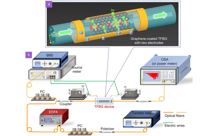
Figure 1(a) schematically depicts the structure of the in-fiber photoelectric device with graphene layer and a pair of electrodes. The grating planes of the TFBGs were inscribed with a predefined tilt relative to the fiber axis, which could promote the light coupling from the core to cladding modes and excite a series of comb-like resonances in a wide spectrum range of tens to hundreds of nanometers. The resonant cladding modes can be partially absorbed by graphene layer to yield the photocurrent, and be further detected by a pair of “L-shaped” electrodes and a source meter. In order to improve the light absorption of graphene layer, from Fig. 1(a), the graphene layer is transferred to the light-coupled direction (orientation of grating planes) from the fiber core, in which relatively stronger evanescent field will leak out. Whereas, the two symmetric long electrodes are placed in parallel on both sides of graphene layer to receive the photocurrent.

Figure 1.(a) Schematic of the configuration and operation principle of the graphene-coated TFBG integrated with a pair of electrodes. (b) Experimental arrangement for measuring the transmission spectrum and photoelectric conversion performance of the TFBG device. BBS, broadband light source; PC, polarization controller; EDFA, Erbium-doped fiber amplifier; OSA, optical spectrum analyzer.
Figure 1(b) shows the experimental system for measuring the transmission spectrum, photoelectric and electro-optical conversion performance of the TFBG device. The broadband light source (BBS) and optical spectrum analyzer (OSA) are used to observe the change of spectral characteristics and track the transmission dips of the cladding modes. The narrowband probe light was supplied by an amplified tunable laser (TL) with an erbium-doped optical fiber amplifier (EDFA) and modulated by a polarizer and polarization controller (PC), and then the photoelectric conversion performance by absorbing evanescent field of TFBG at the graphene layer was characterized by a source meter. During the photoelectric testing, the BBS could be removed to ensure the detection of light at a specific wavelength and eliminate the effect of background light. Both the converted electric signal and transmitted optical signal were simultaneously recorded and analyzed by the source meter and a power meter (instead of the OSA) in real time.
The employed TFBG with a tilt angle of 7° was fabricated in commercial single mode fiber (SMF) by using a frequency-doubled continuous wave Ar+ laser and scanning phase-mask technique. The SMF was first hydrogenated to enhance the photosensitivity. A high-quality large-size graphene with a three-layer thickness is coated to provide a stable and uniform absorption layer of the cladding modes. In the device fabrication, a pair of symmetrical gold electrodes should place in the weaker evanescent field direction, which is parallel to the direction of the tilted grating planes, as shown in Fig. 1(a) and the right inset of Fig. 2(a). The diffraction direction was determined and marked in advance by inputting a red laser and rotating the optical fiber. A row of diffraction fringes radiated from the TFBG can be observed when the strong radiation field faces to a whiteboard, by contrast, there is no diffraction pattern radiated out but only a very weak red line in the direction perpendicular to that before, as shown in Fig. 2(b).
Figure 2.(a) Preparation process of the graphene-coated TFBG device and determination of orientations of gold-coating and grating planes. (b) Diffraction fringes at a three-dimensional space, showing the weak and strong evanescent fields at two orthogonal directions, respectively. (c) Optical microscopic images of the device under bright-field, there is the junction of uncoated and coated region between the two electrodes. (d) Raman spectrum of the transferred graphene layer, the G mode is at 1593.19 cm−1.
The integration procedures of two gold electrodes and graphene coating was performed and shown in Fig. 2(a). First, a 5 nm thick chromium layer and a 30 nm thick gold layer were successively deposited on the grating surface by thermal evaporation technique, and the sandwiched chromium underlayer can enhance the surface quality and reliability of the gold electrodes adhesion. Second, the gold and chromium layers towards the marked direction with strong diffraction fringes shown in Fig. 2(a) were manually removed by a piece of thin acrylic sheet with the help of a probe station with high-resolution microscopy, and then a pair of desired and repeatable parallel windows with a length of 10 mm and width of 50 μm were left for graphene coating. During this process, the removal region and direction of the metal layer could be controlled by rotating the fiber device. Third, two channels were scratched on both sides of the grating region to separate from each other and form a pair of symmetrical “L-shaped” electrodes. Finally, an entire piece of graphene film was transferred onto the windows between electrodes by a wetting transfer technique21, 25. The employed few-layer graphene was grown on a copper foil by chemical vapor deposition. After the copper foil was chemically removed by a Fe(NO3)3 solution, the floated graphene film was rinsed with deionized water several times. Then, the fiber grating was immersed into water to pick up the floated graphene film, which was directly coated on the marked regions of the grating surface.
Since the gap width between the two electrodes is an important factor in the photoelectric conversion, we examined it by a high-resolution optical microscope. From Fig. 2(c), the result shows a 44 μm wide window with distinct graphene border, which allows that the evanescent field is concentrated in this region and completely absorbed by the graphene. In order to verify the uniformity of the graphene, we selected multiple points of the transferred graphene film on the TFBG to characterize by a Raman spectrometer. Almost identical Raman spectra were obtained, as shown in Fig. 2(d), including the featured peaks of 1593.19 cm−1 (G band), 2691.94 cm−1 (2D band) as well as 1347.87 cm−1 (D band)20, 26, 27.
For a TFBG, a group of cladding mode resonances and strong evanescent field appear at a densely comb-like wavelength, determined by the phase-matching condition
, where,
is the resonant wavelength of the ith cladding mode, Λ is the nominal grating period, θ is the tilt angle, and
and
are the effective refractive indices of the core mode and the ith-order cladding mode, respectively. Thus, the polarized transmission spectrum and modal field distribution are two important features to trace and understand the light-matter interaction. Figure 3(a)shows the transmission spectra of the employed TFBG before and after integration of the graphene coating and electrodes, under two orthogonal P-polarized and S-polarized light incidences. Clearly, the two polarized cladding mode resonances have some attenuations after transferring the few-layer graphene, and the S-polarized intensity attenuated more than the P-polarized counterpart. This means the graphene layer absorbs more S-polarized mode energy that the electric field direction is parallel to the graphene, in comparison with the P-polarized mode whose electric field is vertical to the graphene. To obtain further insight, we selected one of the cladding modes in the cyan region of Fig. 3(a), and then numerically calculated their electric field distributions by using finite element analysis method. Since cladding modes with different orders at a given polarization state have similar mode field distributions, the simulation results are adapted to other cladding modes. The results are shown in Fig. 3(b) and 3(c). The P- and S-polarized modes have different effective indices of 1.4089–3.69×10⁻⁵ i and 1.4096– 6.45×10⁻⁵ i, indicating the direction of the electric field perpendicular to each other. Figure 3(d) plots the electric field intensity of the modes along radial direction of the fiber, and the inset shows the intensity distribution near the graphene layer. The larger electric field intensity of S-polarized mode in the graphene layer indicates more absorption on the S-polarized modes, which can be also confirmed by the enlarged transmission spectra shown in Fig. 3(e). The polarization-dependent mode field will allow different photoelectric conversion responsivities.
Figure 3.(a) Polarized transmission spectra of the TFBG before and after graphene coating. (b, c) Simulated electric field distributions of the selected P-polarized and S-polarized cladding modes of the graphene-coated TFBG. (d) Electric field intensity of P-polarized and S-polarized modes along the fiber radial. The inset shows the intensity distributions of the 25th-order cladding modes near the boundary between fiber and graphene layer. (e) Enlarged transmission spectra before and after graphene coating.
Photoelectric response
To examine the photoelectric response of the graphene-coated TFBG device, we established the experimental system as shown in Fig. 1(b). In this system, the transmitted spectrum, output power and photocurrent signal can be monitored in real-time. The photocurrent was excited by a pump light generated through a TL at a specific wavelength of cladding mode resonance. The in-line fiber polarizer and PC were used to control the polarization state at S- or P-polarized mode, which were fixed during the examination. The converted photocurrent signal was collected and recorded by a source meter. In the experiment, the gap width of 50 μm between the two electrodes was chosen to ensure the energy of leaked mode field completely absorbed by the graphene layer for high-performance photoelectric conversion.
In the experiment, the P-polarized resonance at 1533.30 nm and S-polarized resonance at 1533.42 nm are selected for photoelectric response test. The results are shown in Fig. 4, and the top and bottom panels correspond to the cases pumped by the P-polarized and S-polarized resonances, respectively. For the case of the P-polarized incidence, the photocurrent Iph=Iillumination−Idark increase linearly with the bias voltage Vbs under different powers absorbed by graphene, as shown in Fig. 4(a). The linear relationship of Iph versus Vbs also confirmed a good ohmic contact between the graphene layer and the two gold electrodes. However, the high bias voltage will increase the dark current and induce the thermal effect. At the same time, the thermally-induced spectral shift of TFBG device will further increase the fluctuation of photocurrent. When a weak incident light power Pgr absorbed by graphene coating, as shown in the inset of Fig. 4(b), the photocurrent increases linearly and rapidly with the incident power in the beginning. Also from Fig. 4(b), with the further increase of the incident power, the change of photocurrent gradually slows down especially after 50 μW, and then the photocurrent trends to saturation around 80 μA. From Fig. 4(c), the responsivity (defined as Iph/Pgr) decreases as the incident power Pgr increases, and for a weak incident power, there is a negative exponential relationship between the responsibility and incident power under a bias voltage of 0.3 V. The maximum responsivity is up to 11.4 A/W when the incident power is 0.16 μW. With the incident power Pgr over 2.0 μW, the responsibility keeps almost unchanged at around 7.0 A/W.
Figure 4.Photoelectric response of the graphene-coated TFBG device. (a, b) Dependence of photocurrent on the power absorbed by graphene with P-polarized light pump under applied bias voltages of 0.1, 0.2 and 0.3 V, and (c) photoelectric responsivity of the device changing with the incident power at a bias voltage of 0.3 V. The inset of (b) shows the linear power-dependence of photocurrent in the low-power case. The inset of (c) shows the operation mechanism of electron-hole pair excitation in graphene in weak light (left) and saturated absorption (right). (d–f) Power-dependence and responsivity of the photocurrent for the case of S-polarized light pump.
As a comparison, the examination results for the case of S-polarized incidence are shown in Fig. 4(d–f). It can be seen that the photocurrent Iph still increase linearly with the bias voltage Vbs at different incident powers absorbed by graphene, and present a similar growth trend with the incident power. However, the saturation photocurrent is up to 100 μA, and the maximum photoresponsivity is 5.2 A/W. Due to that the responsivity decreases as the increase of incident power, the more absorption of S-polarized light by graphene layer results in the lower responsivity and higher saturation photocurrent in comparison with the case of the P-polarized incidence, as shown in Fig. 4(d) and 4(f), which agree well with the previous reports28-30.
Benefitting from the long interaction length (~10 mm), large absorption area and almost no decaying evanescent field around TFBG, the high saturation photocurrent is obtained in both polarizations. This saturation phenomenon of the photocurrent can be explained from the insets of Fig. 4(c). The interband transition of carriers will occur for a weak light absorbed by graphene31. Whereas, as the incident power further increase, the conduction and valence bands will be fully filled by the photogenerated carriers, preventing the further absorption, as shown in the right inset of Fig. 4(c). As a result, the photocurrent will grow more and more slowly and tend to be saturated, and the responsivity will keep unchanged with the increase of the incident power.
Due to the densely comb-like spectral characteristics of TFBG, it is specifically described as the intensity of evanescent field is strongly wavelength-dependent. The light power absorbed by graphene layer is accordingly determined by the spectral comb. When the incident light is approaching to the resonant wavelength of TFBG, a strong photoelectric conversion occurs. When the incident wavelength is away from the resonant wavelength, there is almost no photocurrent generation. Figure 5(a) demonstrates the wavelength-dependence of the photocurrent (blue solid-line) and the transmission (red dashed-line) in the wavelength range of 1510–1520 nm. The transmission was monitored by a tunable laser and a commercial photodetector, and the photocurrent was then collected by the source meter. From Fig. 5(a), the photocurrent evolution with the wavelength agrees well with the transmission of the device, and the maximum photocurrent appears at the resonant dips in which the cladding mode intensity is more coupled to the graphene layer. Moreover, the photocurrent curve demonstrates higher measurement resolution and gives more spectrum details than the transmission. Therefore, the device can be used as a fiber-based micro-spectrometer, and the operation wavelength is strongly determined by the range of cladding mode resonance.
Figure 5.(a) Wavelength dependence (blue solid-line) of the photocurrent, which is well-matched with the transmission (red dashed-line) of TFBG scanned with a TL and measured with a commercial photodetector. (b) Temporal response of TFBG-based photodetector. (c) Temporal responses of the photodetector at different applied voltages with a fixed light power.
To evaluate the dynamic response of the device, we periodically switched the incident light signal with an acousto-optic modulator at a bias voltage of 1.0 V, and the output photocurrent is shown in Fig. 5(b). The calculated rising time and falling time are 196 ms and 188 ms, respectively, following by the 10%–90% definition in analog signal processing. In addition, we supplied different bias voltages of 0.1, 0.5, 1, 1.5 and 2 V to test the responsivity. Clearly, the photocurrent increases accordingly with the bias voltage, indicating a good stability and repeatability. Still, there is a challenge in the improvement of the response speed due to the long light-matter interaction length and the integrity and homogeneity of graphene layer in such a large area.
Electrically-induced thermo-optic response
For the graphene-coated TFBG, when an electrical signal is applied on the graphene layer, the spectrum of the TFBG will appear a global red-shift due to the electrically pumped Joule heating effect. Determined by the thermo-optic and thermal expansion effects32-34, the spectral shift Δλ with the change ΔT of ambient temperature can be expressed as Δλ/λ=(α+ζ)ΔT, where α=1/neff · dneff/dT and ζ=1/Λ · dΛ/dT are the coefficients of the thermo-optic and thermal expansion, and λ is the resonant wavelength of a specific cladding mode. For the device, the graphene layer can be regarded as a pellet resistance R, and the generated Joule heating Q is proportional to the square of current I2, Q=I2R. Therefore, the spectral shift can sense the injected current and has a linear response with the square current.
To confirm this, another similar TFBG device with graphene coating and a pair of gold electrodes on both sides was fabricated, and the transmission spectrum is shown in Fig. 6(a). In the experiment, we remove one incident light including the TL, polarizer, PC and EDFA shown in Fig. 1(b), and apply an adjustable current signal on the TFBG using two tungsten needles and the high-precision source meter. Launched from the BBS, the transmission spectrum of TFBG is still recorded by the OSA. The results show that the transmission spectrum has a global red-shift with the increase of the injected current. To clearly observe the spectral shift shown in Fig. 6(a), we depicted the evolution of one (Dip A) of cladding mode resonances in the spectrum with the increase of current from 0 to 2.85 mA, demonstrating a red-shift of 0.17 nm, as shown in Fig. 6(b). Also, the resonant wavelength of the cladding mode linearly shifts with the square current of 0–8 mA2, and the linear response coefficient is 2.167×10⁴ nm/A2 with a correlation coefficient R2 of more than 0.999, as shown in Fig. 6(c). The strictly linear relationship originates from the electrically generated Joule heating proportional to the square of current and relatively perfect graphene integration without energy loss during current conduction35, 36. However, as the applied current further increases, the generation and dissipation of heat will gradually reach equilibrium, then the transmission spectrum trends to be stable22. In addition, the electrically-induced shift of the resonance dip in the current range of 0–2.85 mA could provide a thermal-optic switching effect.
Figure 6.(a) Transmission spectrum of the graphene-coated TFBG. (b) Spectral shift of one (Dip A) of the cladding modes with the increase of current. (c) Wavelength shift versus the square of current. (d) Measured transmission spectra of the TFBG without (red) and with (blue) the electrical injection of 2.85 mA, and the spectrum of a switching signal light. (e) Temporal response of the “electric-optical” switching effect. (f) Enlarged temporal response over a period with a rise/fall time of 148 ms/56 ms.
To examine the response speed, the graphene-coated TFBG was used as a filter to modulate or switch a signal light from the TL, as shown in Fig. 1(b). In the measurement, the TL was set at 1538.24 nm as a signal source, and the modulated signal was tracked by a photodetector and an oscilloscope in real-time. When turning on or off the applied current of 2.85 mA on the graphene layer, the TFBG’s mode resonance will have a fast shift from the “peak” to “dip” at the wavelength of the signal light, corresponding to “on” and “off” states of the signal, as shown in Fig. 6(d). The periodical change of the signal is shown in Fig. 6(e), when a square-wave modulated voltage is applied with a duty cycle of 0.9 s∶0.6 s. The dynamic response results indicate the good stability and repeatability of the device in multiple periods. As shown in Fig. 6(f), the times taken for the rising and falling edges of the signal are evaluated as 148 ms and 56 ms, respectively, following the 10%–90% rule of analog signal processing.
From the above results, the graphene layer as a source of electric-induced heat generation in this device, has a uniform, fast and stable heating manner without no loss and delay to modulate the spectral characteristics of a TFBG, due to the tight wrapping of graphene around the TFBG. In the previous works, the copper or chrome-nickel wires were employed to heat the microfibers for phase/wavelength modulating and current sensing37-40, demonstrating low thermal/current sensitivity or response speed as a result of the small contact area or inhomogeneous heating manner with possible gaps. For instance, by using the copper rod as a heating element, the wavelength of microfiber knot resonator shifted with the square current, with a response coefficient of 700 pm/A237. By wrapping a microfiber on a thin-diameter chromium-nickel wire to construct a microfiber loop resonator based current sensor, the current sensitivity was up to 220.65 nm/A238. A power resistor around a tapered fiber interferometer was used to heat the interference region, and the current sensitivity was only 1.76 nm/A239. A microfiber interferometer was placed in contact with a copper wire carrying a direct current to be used as a current sensor, the sensitivity and response time were only 48.18 pm/A2 and around 6.4 s, respectively40. In addition, with the aim of the current sensing, the use of the optical micro/nanofiber-based Mach-Zehnder interferometers40-43, resonators36, 44, increase the risk of instability and susceptibility to the environmental disturbance. As a comparison, the response sensitivity is improved by more than two orders of magnitude in our device, and the speed and stability also have a great enhancement by using the electrically-pumped graphene-coated TFBG scheme.
Conclusions
We have demonstrated the achievement of photoelectric conversion and electrically-induced thermo-optic effect in an in-fiber device assisted by the graphene layer and two symmetrical electrodes. In the device, a TFBG is used to provide a strong evanescent field and a multiresonant spectrum characteristics, and the few-layer graphene acts as a photoelectric conversion medium as well as a microheater by the electrical injection. For the photocurrent generation, the device shows a wavelength- and polarization-dependent photoresponse with responsivity up to 11.4 A/W, saturation photocurrent of around 100 μA and response speed of 196 ms. For the electrically-induced thermal effect, the wavelength shift can reach 0.17 nm at the applied current of 2.85 mA, and the response time and maximal extinction ratio of the thermal-optical switch are 148 ms and 15 dB, respectively, due to the long-distance, homogeneous heat generation and transfer of graphene layer. Moreover, the use of reduced-diameter fiber, the grating with a larger tilt angle, and more homogenous monolayer graphene directly grown on the fiber device by chemical vapor deposition technique, would further promote the improvement of the photoelectric performance. Therefore, with the advantages of all-fiber system, the propagation, filtering, modulation, and detection of the light signal can be realized in a fiber device without loss for integration, which is more flexible than using lens system and fiber coupling system to focus the light source into on-chip waveguide. This work also provides a potential pathway to develop multifunctional fiber-based photoelectric device with 2D material integration.
Acknowledgements
We are grateful for financial supports from National Natural Science Foundation of China (Grant No. 61975166) and Key Research and Development Program (Grant No. 2022YFA1404800). We also thank the Analytical & Testing Center of NPU for their assistance with the material and device characterizations.
BQ Jiang and XT Gan proposed the original idea. YG Hou fabricated the sample and performed the measurements, assisted by JX Wu and YX Ma. BQ Jiang and YG Hou wrote the original manuscript, XT Gan and JLZhao revised it. BQ Jiang, XT Gan and JL Zhao provided resource support and supervised the project.
The authors declare no competing financial interests.
References
[1] JH Chen, Q Jing, F Xu, ZD Lu, YQ Lu. High-sensitivity optical-fiber-compatible photodetector with an integrated CsPbBr3-graphene hybrid structure. Optica, 4, 835-838(2017).
[2] YF Xiong, F Xu. Multifunctional integration on optical fiber tips: challenges and opportunities. Adv Photon, 2, 064001(2020).
[3] M Principe, M Consales, A Micco, A Crescitelli, G Castaldi et al. Optical fiber meta-tips. Light Sci Appl, 6, e16226(2017).
[4] Z Hao, BQ Jiang, YX Ma, RX Yi, XT Gan et al. Broadband and continuous wave pumped second-harmonic generation from microfiber coated with layered GaSe crystal. Opto-Electron Adv, 6, 230012(2023).
[5] Z Hao, YX Ma, BQ Jiang, YG Hou, AL Li et al. Second harmonic generation in a hollow-core fiber filled with GaSe nanosheets. Sci China Inf Sci, 65, 162403(2022).
[6] LQ Zhuo, PP Fan, S Zhang, YS Zhan, YM Lin et al. High-performance fiber-integrated multifunctional graphene-optoelectronic device with photoelectric detection and optic-phase modulation. Photon Res, 8, 1949-1957(2020).
[7] JH Chen, YF Xiong, F Xu, YQ Lu. Silica optical fiber integrated with two-dimensional materials: towards opto-electro-mechanical technology. Light Sci Appl, 10, 78(2021).
[8] F Chiavaioli, D Santano Rivero, I Del Villar, AB Socorro-Leránoz, XJ Zhang et al. Ultrahigh sensitive detection of Tau protein as Alzheimer's biomarker via microfluidics and nanofunctionalized optical fiber sensors. Adv Photonics Res, 3, 2200044(2022).
[9] F Chiavaioli, P Zubiate, I Del Villar, CR Zamarreño, A Giannetti et al. Femtomolar detection by nanocoated fiber label-free biosensors. ACS Sens, 3, 936-943(2018).
[10] KO Hill, Y Fujii, DC Johnson, BS Kawasaki. Photosensitivity in optical fiber waveguides: application to reflection filter fabrication. Appl Phys Lett, 32, 647-649(1978).
[11] T Erdogan, JE Sipe. Tilted fiber phase gratings. J Opt Soc Am A, 13, 296-313(1996).
[12] A Wolf, A Dostovalov, K Bronnikov, M Skvortsov, S Wabnitz et al. Advances in femtosecond laser direct writing of fiber Bragg gratings in multicore fibers: technology, sensor and laser applications. Opto-Electron Adv, 5, 210055(2022).
[13] C Caucheteur, T Guo, J Albert. Multiresonant fiber gratings. Opt Photonics News, 33, 42-49(2022).
[14] BQ Jiang, JL Zhao. Nanomaterial-functionalized tilted fiber gratings for optical modulation and sensing. J Lightwave Technol, 41, 4103-4113(2023).
[15] YZ Sun, ZJ Yan, KM Zhou, BB Luo, BQ Jiang et al. Excessively tilted fiber grating sensors. J Lightwave Technol, 39, 3761-3770(2021).
[16] XT Gan, D Englund, D Van Thourhout, JL Zhao. 2D materials-enabled optical modulators: from visible to terahertz spectral range. Appl Phys Rev, 9, 021302(2022).
[17] SQ Yan, Y Zuo, SS Xiao, LK Oxenløwe, YH Ding. Graphene photodetector employing double slot structure with enhanced responsivity and large bandwidth. Opto-Electron Adv, 5, 210159(2022).
[18] JH Chen, BC Zheng, GH Shao, SJ Ge, F Xu et al. An all-optical modulator based on a stereo graphene-microfiber structure. Light Sci Appl, 4, e360(2015).
[19] SL Yu, XQ Wu, KR Chen, GB Chen, X Guo et al. All-optical graphene modulator based on optical Kerr phase shift. Optica, 3, 541-544(2016).
[20] QL Bao, H Zhang, B Wang, ZH Ni, CHYX Lim et al. Broadband graphene polarizer. Nat Photonics, 5, 411-415(2011).
[21] BQ Jiang, GL Yin, KM Zhou, CL Wang, XT Gan et al. Graphene-induced unique polarization tuning properties of excessively tilted fiber grating. Opt Lett, 41, 5450-5453(2016).
[22] BQ Jiang, YG Hou, HY Wang, XT Gan, AL Li et al. Few-layer graphene integrated tilted fiber grating for all-optical switching. J Lightwave Technol, 39, 1477-1482(2021).
[23] XT Gan, CY Zhao, YD Wang, D Mao, L Fang et al. Graphene-assisted all-fiber phase shifter and switching. Optica, 2, 468-471(2015).
[24] BQ Jiang, XM Zhang, AL Li, YG Hou, Z Hao et al. Electrically induced dynamic Fano-like resonance in a graphene-coated fiber grating. Photonics Res, 10, 05001238(2022).
[25] BQ Jiang, X Lu, XT Gan, M Qi, YD Wang et al. Graphene-coated tilted fiber-Bragg grating for enhanced sensing in low-refractive-index region. Opt Lett, 40, 3994-3997(2015).
[26] M Qi, YX Zhou, FR Hu, XL Xu, WL Li et al. Improving terahertz sheet conductivity of graphene films synthesized by atmospheric pressure chemical vapor deposition with acetylene. J Phys Chem C, 118, 15054-15060(2014).
[27] AC Ferrari. Raman spectroscopy of graphene and graphite: disorder, electron–phonon coupling, doping and nonadiabatic effects. Solid State Commun, 143, 47-57(2007).
[28] P Ma, Y Salamin, B Baeuerle, A Josten, W Heni et al. Plasmonically enhanced graphene photodetector featuring 100 Gbit/s data reception, high responsivity, and compact size. ACS Photonics, 6, 154-161(2019).
[29] E Khosravian, HR Mashayekhi, A Farmani. Highly polarization-sensitive, broadband, low dark current, high responsivity graphene-based photodetector utilizing a metal nano-grating at telecommunication wavelengths. J Opt Soc Am B, 38, 1192-1199(2021).
[30] LX Sun, YQ Zhang, YJ Wang, Y Yang, CL Zhang et al. Real-time subcellular imaging based on graphene biosensors. Nanoscale, 10, 1759-1765(2018).
[31] QL Bao, H Zhang, Y Wang, ZH Ni, YL Yan et al. Atomic-layer graphene as a saturable absorber for ultrafast pulsed lasers. Adv Funct Mater, 19, 3077-3083(2009).
[32] Z Li, YG Xiao, F Liu, XY Yan, DT You et al. Operando optical fiber monitoring of nanoscale and fast temperature changes during photo-electrocatalytic reactions. Light Sci Appl, 11, 220(2022).
[33] J Albert, LY Shao, C Caucheteur. Tilted fiber Bragg grating sensors. Laser Photonics Rev, 7, 83-108(2013).
[34] SE Kipriksiz, M Yücel. Tilted fiber Bragg grating design for a simultaneous measurement of temperature and strain. Opt Quant Electron, 53, 6(2021).
[35] Y Cheng, G Cui, CH Liu, ZT Liu, LG Yan et al. Electric current aligning component units during graphene fiber Joule heating. Adv Funct Mater, 32, 2103493(2022).
[36] SC Yan, BC Zheng, JH Chen, F Xu, YQ Lu. Optical electrical current sensor utilizing a graphene-microfiber-integrated coil resonator. Appl Phys Lett, 107, 053502(2015).
[37] A Sulaiman, SW Harun, F Ahmad, SF Norizan, H Ahmad. Electrically tunable microfiber knot resonator based erbium-doped fiber laser. IEEE J Quantum Electron, 48, 443-446(2012).
[38] XD Xie, J Li, LP Sun, X Shen, L Jin et al. A high-sensitivity current sensor utilizing CrNi wire and microfiber coils. Sensors, 14, 8423-8429(2014).
[39] R K, N Kumar, V Sahoo. A highly accurate all-fiber MMZI current sensor. IEEE Sens J, 15, 1270-1274(2015).
[40] AA Jasim, J Faruki, MF Ismail, H Ahmad. Fabrication and characterization of microbent inline microfiber interferometer for compact temperature and current sensing applications. J Lightwave Technol, 35, 2150-2155(2017).
[41] A Sulaiman, SW Harun, I Aryangar, H Ahmad. DC current sensing capability of microfibre Mach-Zehnder interferometer. Electron Lett, 48, 943-945(2012).
[42] AA Jasim, SW Harun, MZ Muhammad, H Arof, H Ahmad. Current sensor based on inline microfiber Mach–Zehnder interferometer. Sens Actuators A Phys, 192, 9-12(2013).
[43] S Nodehi, WS Mohammed, H Ahmad, SW Harun. Realization of spectral tunable filter based on thermal effect in microfiber structure. Opt Fiber Technol, 28, 38-41(2016).
[44] GY Chen, G Brambilla, TP Newson. Inspection of electrical wires for insulation faults and current surges using sliding temperature sensor based on optical Microfibre coil resonator. Electron Lett, 49, 46-47(2013).