Abstract
A mode-locked (ML) picosecond ytterbium-doped thin disk laser using a monolayer as the saturable absorber (SA) is demonstrated. The monolayer is fabricated through the method of low-pressure chemical vapor deposition. The laser directly produces stable ML picosecond pulses at a slope efficiency of 9.71%. The maximum output power is approximately 890 mW, while the corresponding repetition, pulse energy, and pulse duration are 48.6 MHz, 18.3 nJ, and 13.1 ps, respectively. Results suggest that the monolayer is a promising SA for ultrafast lasers system.An ultrafast laser source has attracted great interest over the past few decades as the average output power and pulse energy for ultrafast lasers have grown remarkably, paving the way for a variety of applications[1,2]. High-power picosecond sources are especially attractive to the application of photocathode radio frequency (RF) guns, -ray generation using inverse compton scattering, and optical parametric chirped-pulse amplification (OPCPA)[3–5], as the development of secondary sources become critical to these kinds of applications. The typical operating points are in the 1–20 ps laser pulse duration regime[6]. So far, average power scaling has been demonstrated with multipass megahertz (MHz) amplifiers[7], as well as oscillators[1,8,9]. For some experiments, such as cold target recoil ion momentum spectroscopy (COLTRIMS), time-resolved photoemission electron microscopy (PEEM), and femtosecond electron diffraction, the output from high-power MHz-repetition-rate oscillators can improve the signal-to-noise ratio significantly[10]. Because of these properties, MHz-repetition-rate high-power oscillators are highly preferred[11]. Nowadays leading thin-disk (TD) technology has been developed unprecedented thanks to its unique aspect ratio as well as thermal management[12], and the property of high intracavity peak power makes TD architecture a good candidate for mode-locking lasers.
Recently, intense research has been applied in the field of low dimensional nanomaterials. It has been reported that two-dimensional (2D) and quasi-2D nanomaterials, such as monolayer and few-layer graphene exhibit attractive optical and electrical properties[13] like ultrafast photo response and ultra-wideband response ranging from ultraviolet to terahertz[14]. Despite those merits, graphene is also born with two intrinsic disadvantages: zero band-gap and weak absorption coefficiency. In addition to carbon based 2D materials, atomic layer transition metal dichalcogenides (TMDs) are currently under special attention due to their unique optical properties that may complement graphene. , one typically excellent material of TMDs, has a thickness-dependent electronic and optical property. That is, monolayer or few-layer turns out to be a direct band-gap semiconductor with enhanced light activity[15]. Its thickness-dependent band-gap and electronic band structure ensures the new optical properties, which are distinct from graphene[16,17]. When concerning the third-order nonlinear optical response based on recent findings by various research groups, few-layer and monolayer had been ambiguously verified to exhibit enhanced optical saturable absorption (SA), owing to its semiconducting property[18,19]. Few-layer or monolayer could play a significant role in future optoelectronic and photonic technologies[20,21], particularly as a wideband SA for a versatile pulsed laser source[14].
In this Letter, we combine the merit of high intracavity intensity of a TD laser (TDL), as well as the unique optical and electrical properties of , and demonstrate a stable mode-locked (ML) picosecond ytterbium-doped TDL using a monolayer as the SA. The laser produces ML picosecond pulses with a slope efficiency of 9.71%, a maximum output power of 890 mW, and a corresponding frequency, pulse energy, and pulse duration of 48.6 MHz, 18.3 nJ, and 13.1 ps, respectively. To the best of our knowledge, this is the first time that is applied as an SA in Yb:YAG TD continuous wave ML (CWML) lasers. In addition, the average power and pulse energy indicate that is a promising SA for an ultrafast solid state laser.
Sign up for Chinese Optics Letters TOC. Get the latest issue of Chinese Optics Letters delivered right to you!Sign up now
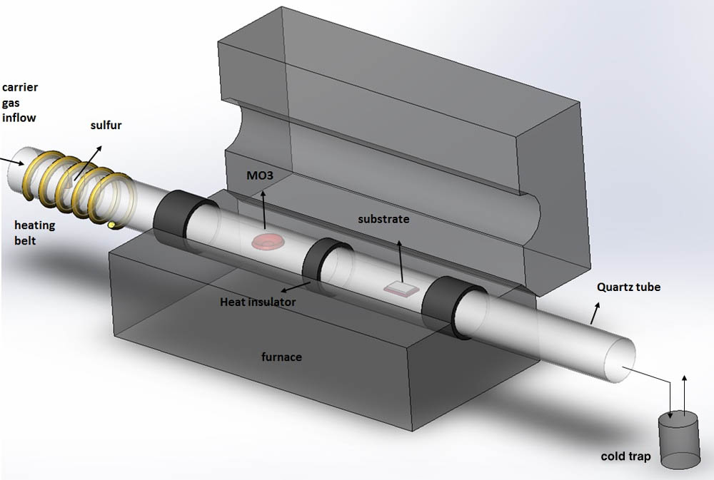
The monolayer sample and the data of the membrane used in our experiment are provided by 6carbon technology (Shenzhen). The membrane is fabricated through the method of low-pressure chemical vapor deposition (LPCVD) technology[22], and Fig. 1 presents the experimental setup for the fabrication of the membrane. The system is made up of six parts: a multi-temperature-zone furnace for heating, a quartz tube for the flow of the gas, an upstream heating belt to evaporate the chalcogen powders, three heat insulators to prevent the thermal from diffusion in a different reaction section, a cold trap placed for solidification of reactive species in the outflow, and a mechanical pump installed downstream to exhaust the outflow and maintain low pressure of the growth system. When considering the reaction between gaseous Mo and S, the process can be described as follows: first, powder and a suitable growth substrate, such as , are positioned in the upstream and downstream sections of the quartz tube, respectively. Then, the is partially reduced by gaseous S to form a volatile species. Afterwards, the species are subsequently conveyed downstream by the carrier gas, and it reacts with S to deposit on the substrate. Pressure of different reactive places can be optimized by controlling the evaporation temperature of S and , which will influence the deposition progress on the substrate. By carefully tuning the temperature of different reaction sections and the reaction time of the chemical vapor deposition, the desired on the substrate can be achieved.

Figure 1.Setup of our LPCVD system to fabricate an membrane.
The optical microscopic picture of monolayer continuous film on the wafer is displayed in Fig. 2(a). The picture indicates that the sample has a relatively large specific surface area. A transparency spectrum of the film is illustrated in Fig. 2(b), where the absorption peaks are located at the 250–260 and 400–450 nm regions, which have the general features coinciding with that of the 2D nano-system with trigonal prismatic coordination, implying that the nano-sheets are a 2 H polytype[23]. The Raman spectrum is performed to identify the atomic structural arrangement of the membrane, as shown in Fig. 2(c), where two characteristic peaks are centered at 385.1 and , which correspond to the in-plane and out-of-plane vibration mode of the hexagonal [24], respectively. The mean frequency difference is calculated to be about . It has been reported that Raman spectroscopy can be applied to verify the number of layers in few-layer or monolayer crystals based on the two peaks and the energy difference value between the two peaks[24]. Through analysis, we can conclude that in our case the synthesized film is mainly made up of a monolayer. In addition, the photoluminescence (PL) spectrum of the film is presented in Fig. 2(d), where the fluorescence radiation peaks are mainly located in the region of 600–700 nm. We used a transmission method to measure the SA of the sample, and a commercial femtosecond () solid state laser at 1030 nm with a repetition of was used as the input laser source. The power-dependent absorption measurement was carried out by changing the power of the seed laser. To obtain the nonlinear optical parameters, a simple SA model of [22] was introduced to fit the measured data. , , , , and correspond to the transmission, modulation depth, input intensity, saturation intensity, and non-saturable loss, respectively. As shown in Fig. 3, the modulation depth, non-saturable loss, and saturation intensity were obtained to be 6.0%, 3.5%, and , respectively.
Figure 2.(a) The optical microscopic picture of a monolayer continuous film on an wafer, (b) transparency spectrum of film, (c) Raman spectrum of a monolayer , and (d) PL data of monolayer .
Figure 3.Nonlinear absorption of the monolayer SA.
Figure 4.Layout of the Yb:YAG CWML TDL system.
The experimental setup of our passively CWML Yb:YAG TDL with as the SA is illustrated in Fig. 4. A 7 a.t.% doped Yb:YAG crystal with a diameter of 12 mm and thickness of 215 μm is used as the gain material. The front surface of the crystal is coated with an antireflection film for 940 nm as well as 1030 nm and with a high-reflection (HR) film for 940 and 1030 nm on the other surface. The TD crystal as well as the pump module is provided by GmbH. The disk is cooled down with an anti-corrosion solution from Opti Temp Inc. at a temperature of 20°C. The crystal is pumped by a 940 nm laser diode with core diameter of 600 μm and the , while the pump beam diameter is set to be 3.2 mm on the crystal.
The layout of the Yb:YAG CWML TDL system is illustrated in Fig. 4, where C1 and C2 correspond to the TD crystal, M1 is an output coupler, and M2–M6 is the HR mirror for 1030 nm. Without considering the thermal lens effect, the radii curvature of the crystal surface is about 7.4 m. The transmission and radii curvature for coupler M1 is 5% and 5 m, respectively. For the high-reflective mirrors M2–M6, the corresponding radii curvature is infinite, infinite, 5 m, 0.2 m, and infinite, respectively. The beam radius evolution inside the cavity is presented in Fig. 5, where , , , , and , and L1 is the length between coupler M1 and crystal C1, L2 is the length between laser pass through the TD crystal for the first and second times, L3 is the length between crystal C2 and M4, L4 is the length between M4 and M5, and L5 stands for the length between M5 and M6. In Fig. 5, T and S stand for the beam diameter evolution in the tangential and sagittal plane, respectively. The beam diameter on the TD crystal is about 2.4 mm, which is a little smaller than 0.8 times of the pump diameter, so a comparably excellent beam profile can be achieved[25]. In our CWML experiment, the membrane SA is placed closed to the flat end mirror M6.
Figure 5.Cavity design of the disk-based oscillator using a double pass on the disk. M1, M4, M5, and M6, mirrors; C1 and C2, crystal.
The pump beam is collimated to the TD crystal through a TDM 1.0 HP module from GmbH. The cavity is designed to for 12 passes. Through simulation, we know that after 12 V-shape passes through the TD crystal, more than 90% of the pump energy is absorbed by the TD crystal, where only a 1.5% absorption increase can be observed with increases of reflection times of up to 24 times, as shown in Fig. 6. Typically for a TD crystal with a thickness of 200 μm, the pump module with 12 reflection times is enough. The average output power versus the absorbed power for continuous waves (CWs) as well as passively CWML Yb:YAG TDLs are demonstrated in Fig. 7. The difference between CW operation and CWML operation is that the monolayer is absent in the CW operation. We find that the TDL operated in two distinct ways in the absorbed pump power regions of 28–36 and 36-42 W in the CW mode and the efficiency of the latter region is higher than the previous one. We believe that the unique optical property was probably introduced by the behavior of laser reabsorption in weak pump power. For the CWML mode, the CWML operation established that when the absorbed power reached 32 W, the slope efficiency of the Yb:YAG TDL decreased to 9.7% in the CWML operation, and the decreased slope efficiency included the insertion loss introduced by . The maximum output power for the CWML operation is 0.89 W, corresponding to an absorbed pump power of 42 W. The maximum output power in the CWML operation is restricted by the damage threshold as well as the dimensions of the monolayer membrane.
Figure 6.TD absorption versus reflection times.
Figure 7.Average output power versus absorbed power.
In the experiment of CWML, we first set the pump power to be 35 W and adjusted the end mirror pair to make sure the cavity is operated in the best situation. Then, we inserted the film into the cavity close to flat end mirror M6. Afterwards, we optimized the end mirror so that the laser oscillated inside the cavity, where we then carefully moved the position of the membrane until we found a suitable position on which CWML operation could be established. The CWML pulse sequence at the output power of 890 mW is illustrated in Fig. 8. The pulse train is presented with the distinct divisions, including 1 μs/div [Fig. 7(a)] and 40 ns/div [Fig. 7(b)], and the frequency of the pulse train is 48.6 MHz. The spectra of the CW and CWML operations are measured by using a spectrometer (Ocean optics, HR ) with a resolution of 0.2 nm. As shown in Fig. 9(a), the full width half-maximum of the CWML laser is about 2.12 nm with a center wavelength of 1031 nm. Compared with the CW operation, the spectrum is slightly broadened and shifted to a shorter wavelength. The possible reasons for the phenomenon include different thermal effects as well as a large nonlinear phase based on the higher peak power[26]. We also find a decrease of intensity in the middle of the spectrum in the CWML mode. This phenomenon can be attributed to the effect of hole burning in the limited gain bandwidth. The autocorrelation trace of the CWML laser is collected through an autocorrelator (APE, pulseCheck USB). The pulse duration is about 13.1 ps, which is assumed to be Gauss fitting, as is illustrated in Fig. 9(b). The pulse energy and peak power are estimated to be 18.3 nJ and 1.33 kW by an average output power of 890 mW. In more than 2 h, the stable CWML laser is always presenting. The time-bandwidth product is , because at present the dispersion inside the cavity is not fully compensated through the effect of self-phase modulation. But, the time-bandwidth product of 4.2 showed that a further compressed pulse could be desired with improvement of the experiment.
Figure 8.ML pulse train with different divisions: (a) 1 μs/division; (b) 40 ns/division.
Figure 9.(a) Spectrum of the CW and ML operation; (b) autocorrelation curve as well as the gauss fitted curve for the output pulse with an output power of 890 mW.
In conclusion, a monolayer membrane fabricated through the method of LPCVD is utilized as SA in our experiment. Its ultrafast photo response, ultra-wideband response, thickness-dependent band-gap, and electronic band structure ensures the generation of ultrashort pulses. We combine the merits of high intracavity intensity of the TDL as well as the unique optical and electrical properties of , and for the first time, to the best of our knowledge, demonstrate an ML picosecond ytterbium-doped TDL using a monolayer as the SA. A laser pulse duration of 13.1 ps is obtained with an average power, pulse energy, peak power, and repetition of 890 mW, 18.3 nJ, 1.33 kW, and 48.6 MHz, respectively. In the next step, we will try an membrane that is fabricated through the method of evanescent field interaction as the SA, which can promise a higher damage threshold[27]. With larger scale monolayer TMDs with a higher damage threshold available, perhaps the theory of power scaling in a TDL can be utilized in those kinds of CWML lasers.
References
[1] J. Brons, V. Pervak, E. Fedulova, D. Bauer, D. Sutter, V. Kalashnikov, A. Apolonskiy, O. Pronin, F. Krausz. Opt. Lett., 39, 6442(2014).
[2] A. Diebold, F. Emaury, C. Schriber, M. Golling, C. J. Saraceno, T. Südmeyer, U. Keller. Opt. Lett., 38, 3842(2013).
[3] C.-L. Chang, P. Krogen, K.-H. Hong, L. E. Zapata, J. Moses, A.-L. Calendron, H. Liang, C.-J. Lai, G. J. Stein, P. D. Keathley. Opt. Express, 23, 10132(2015).
[4] H. Liang, P. Krogen, R. Grynko, O. Novak, C.-L. Chang, G. J. Stein, D. Weerawarne, B. Shim, F. X. Kärtner, K.-H. Hong. Opt. Lett., 40, 1069(2015).
[5] S. Prinz, M. Haefner, C. Y. Teisset, R. Bessing, K. Michel, Y. Lee, X. T. Geng, S. Kim, D. E. Kim, T. Metzger. Opt. Express, 23, 1388(2015).
[6] J. Pouysegur, F. Guichard, Y. Zaouter, Q. Mocaer, M. Hanna, F. P. Druon, C. Hönninger, E. Mottay, P. Georges. Advanced Solid State Lasers, AM4A.2(2016).
[7] J.-P. Negel, A. Voss, M. A. Ahmed, D. Bauer, D. Sutter, A. Killi, T. Graf. Opt. Lett., 38, 5442(2013).
[8] C. J. Saraceno, F. Emaury, O. H. Heckl, C. R. Baer, M. Hoffmann, C. Schriber, M. Golling, T. Südmeyer, U. Keller. Opt. Express, 20, 23535(2012).
[9] C. J. Saraceno, F. Emaury, C. Schriber, M. Hoffmann, M. Golling, T. Südmeyer, U. Keller. Opt. Lett., 39, 9(2014).
[10] Y. Liu, S. Tschuch, M. Dürr, A. Rudenko, R. Moshammer, J. Ullrich, M. Siegel, U. Morgner. Opt. Express, 15, 18103(2007).
[11] C. Feng, Z. Liu, Z. Cong, X. Xu, J. Xu, H. Rao, F. Bai, P. Li, Q. Wang, J. Fang. Chin. Opt. Lett., 14, 111402(2016).
[12] A. Giesen, H. Hügel, A. Voss, K. Wittig, U. Brauch, H. Opower. Appl. Phys. B, 58, 365(1994).
[13] R. Woodward, R. Howe, G. Hu, F. Torrisi, M. Zhang, T. Hasan, E. Kelleher. Photon. Res., 3, A30(2015).
[14] Z. Zheng, C. Zhao, S. Lu, Y. Chen, Y. Li, H. Zhang, S. Wen. Opt. Express, 20, 23201(2012).
[15] K. F. Mak, C. Lee, J. Hone, J. Shan, T. F. Heinz. Phys. Rev. Lett., 105, 136805(2010).
[16] L. Britnell, R. Ribeiro, A. Eckmann, R. Jalil, B. Belle, A. Mishchenko, Y.-J. Kim, R. Gorbachev, T. Georgiou, S. Morozov. Science, 340, 1311(2013).
[17] A. Carvalho, R. Ribeiro, A. C. Neto. Phys. Rev. B, 88, 115205(2013).
[18] K. Wang, J. Wang, J. Fan, M. Lotya, A. O’Neill, D. Fox, Y. Feng, X. Zhang, B. Jiang, Q. Zhao. ACS Nano, 7, 9260(2013).
[19] H. Zhang, S. Lu, J. Zheng, J. Du, S. Wen, D. Tang, K. Loh. Opt. Express, 22, 7249(2014).
[20] X. Zou, Y. Leng, Y. Li, Y. Feng, P. Zhang, Y. Hang, J. Wang. Chin. Opt. Lett., 13, 081405(2015).
[21] B. Lu, L. Yuan, X. Qi, L. Hou, B. Sun, P. Fu, J. Bai. Chin. Opt. Lett., 14, 071404(2016).
[22] Q. Ji, Y. Zhang, Y. Zhang, Z. Liu. Chem. Soc. Rev., 44, 2587(2015).
[23] R. Wei, H. Zhang, Z. Hu, T. Qiao, X. He, Q. Guo, X. Tian, Z. Chen, J. Qiu. Nanotechnology, 27, 305203(2016).
[24] R. Wei, H. Zhang, X. He, Z. Hu, X. Tian, Q. Xiao, Z. Chen, J. Qiu. Opt. Mater. Express, 5, 1807(2015).
[25] J. Mende, J. Speiser, G. Spindler, W. L. Bohn, A. Giesen. Lasers and Applications in Science and Engineering, 68710M(2008).
[26] L. Kong, G. Xie, P. Yuan, L. Qian, S. Wang, H. Yu, H. Zhang. Photon. Res., 3, A47(2015).
[27] J. Sotor, G. Sobon, K. Grodecki, K. Abramski. Appl. Phys. Lett., 104, 251112(2014).