
Yu Chen, Yang Li, Wenhao Tang, Yutao Tang, Yue Hu, Zixian Hu, Junhong Deng, Kokwai Cheah, Guixin Li. Centimeter scale color printing with grayscale lithography[J]. Advanced Photonics Nexus, 2022, 1(2): 026002
- Advanced Photonics Nexus
- Vol. 1, Issue 2, 026002 (2022)
Abstract
1 Introduction
Compared with the conventional painting technology with chemical dyes, structural color from artificial mediums has broader application ranges and thus becomes a more attractive color management technology.1 It is also environmentally friendly and durable. For some applications, the color management requires a high spectral resolution or a controllable spectral bandwidth. In these scenarios, the design of artificial photonic devices relies on various physical mechanisms such as multilayer interference,2,3 diffraction,4 plasmonic resonance,5
Among various design concepts of the color printing technology, the F–P cavity effect has been attracting scientific attention. Compared with most of the plasmonic and dielectric metasurface devices, colors generated from the F–P cavity usually have less crosstalk. For color printing applications, the reflection23
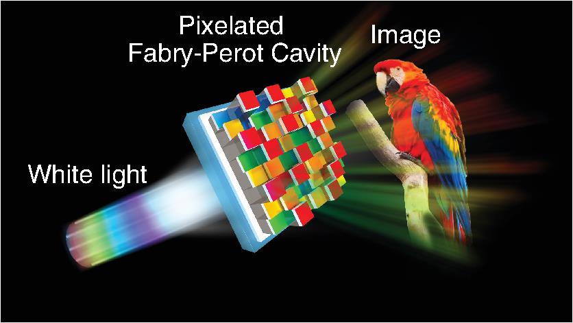
Here, we develop a fast color printing technique by using the concept of pixelated F–P cavities and the laser grayscale lithography process. In this technique, the colorful image with multiple color components is first converted to a predefined grayscale pattern and then engraved on the photoresist (PR) layer by controlling the exposure dose during the grayscale laser writing process. As shown in Fig. 1, the pixelated PR spacer layers are sandwiched by two semitransparent sliver thin films to form the transmission type F–P cavities. Under the illumination of a white light source, the transmission color can be continuously tuned in the visible spectral regime by finely controlling the thickness of the PR layer. We show that a centimeter-scale color printing device with a pixel size of can be fabricated at a record speed of , with a total time of . In the visible regime, the transmission efficiency of the fabricated F–P cavities is between 39% and 50%, which is comparable to that of the EBL-based devices. It should be noted that the pixelated F–P cavity in transmission mode is also an excellent candidate for making color filter arrays, which can be used for spectral imaging. Last, but not least, the large area color filter arrays with various pixel sizes are also demonstrated. It can be found that the newly developed laser grayscale lithography process in this work well leverages the fabrication speed and the spatial resolution of pixelated F–P cavities. All these efforts make it feasible to produce large area and high-resolution color printing devices and color filters for applications in imaging and wearable devices.
Sign up for Advanced Photonics Nexus TOC. Get the latest issue of Advanced Photonics Nexus delivered right to you!Sign up now
![]()
Figure 1.Schematic diagram of the working principle of the color printing by using pixelated F–P cavities. The F–P cavity consists of a silver (Ag)/PR/silver (Ag) sandwich structure. The spatially variant thickness of the PR layer is realized through the laser grayscale lithography process. Under the illumination of a white light source, the colorful image with a micron-scale spatial resolution can be obtained.
2 Results and Discussion
2.1 Calculated Optical Properties of the Fabry–Perot Cavities
Figure 2(a) shows the schematic diagram of the F–P cavity, which consists of a silver (Ag)/ PR/silver (Ag) sandwich structure. The F–P cavity is sitting on a glass substrate. To balance the transmission efficiency and the bandwidth of the transmission peak, the thickness of each silver layer is chosen to be 30 nm. To avoid the oxidation of silver, a encapsulation layer is coated on top of the F–P cavity. To simplify the design and fabrication process, the thickness of the layer, which can affect the transmission property of the cavity, is fixed at 20 nm. Under normal incidence, we numerically calculated the transmission spectra of the F–P cavities with different PR thicknesses. Figure 2(b) shows the typical transmission spectra of the R, G, and B F–P cavities with spacer thicknesses of 138, 105, and 79 nm, respectively. It can be found that the bandwidth of the color filter at longer wavelengths becomes narrower, which is mainly because of the dispersion of silver in the visible spectral region. By scanning the PR thickness from 60 to 160 nm, the resonant wavelengths can be continuously tuned in the visible spectral regime [Fig. 2(c)]. In Fig. 2(d), the colors (black circles), which are calculated from the simulation results in Fig. 2(c), are mapped to the International Commission on Illumination (CIE) 1931 chromaticity diagram. It is shown that the Ag/PR/Ag-based F–P cavities can provide a broadband color range for color printing applications. It should be noted that the transmission peaks will change under oblique incidence;12 however, this is not the focus of the current work.
![]()
Figure 2.Calculated optical responses of the silver (Ag)/PR/silver (Ag) F–P cavities. (a) The cross-section of the F–P cavity. The silver film with a thickness of 30 nm and the PR layer serve as the mirror and the spacer of the F–P cavity, respectively. The F–P cavity sitting on the glass substrate is encapsulated by a 20-nm-thick
2.2 Fabrication and Characterization of the Color Palettes
To experimentally verify the optical properties of the F–P cavities, we fabricate a series of color palettes by using the laser grayscale lithography process (Fig. S5, Supplemental Material). The grayscale photolithography process is based on the commercial direct laser writing equipment from Heidelberg Instruments. The fabrication process includes the following steps: first, a silver layer with a thickness of was deposited on a glass substrate, then the PR layer with a thickness of was spin-coated on top of the silver. The thickness of the spatially variant PR spacer layer can be controlled by varying the exposure dose of a 405 nm laser. After that, the second silver layer with a thickness of 30 nm and a encapsulation layer with a thickness of 20 nm was deposited onto the patterned PR layer by using the electron beam evaporation method.
Then, we characterize the optical performance of the color palettes. As shown in Fig. 3(a), under the illumination of a white light source, the photos of the color palettes with different PR thicknesses are taken by using a Canon camera (Fig. S3, Supplemental Material). The white-balanced photos show that the blue, green, yellow, and red colors can be easily obtained by varying from 83 to 149 nm. In addition, the transmission efficiency of the F–P cavities is summarized in Fig. 3(b). For the F–P cavities working in the visible regime, the transmission efficiencies are between 39% and 50%. It is found that the measured transmission efficiencies are lower than that of calculated ones in Fig. 2. This may be because the imaginary part of the refractive index of the PR used in the numerical model is smaller than that in the real device. The full width at half maximum (FWHM) of the transmission peaks for the red, green, and blue F–P cavities are , 51, and 87 nm, respectively. The bandwidths of the three color filters are narrower than that of commercial products from Thorlabs.32 The calculated transmission efficiency at blue wavelengths is higher than that at longer wavelengths. However, the measured transmission spectra have a reversed trend. This phenomenon should come from the change in the refractive index of the PR layer before and after laser exposure. As demonstrated in Fig. 3(c), the transmission colors of the palettes form a wide gamut in the CIE 1931 chromaticity diagram, which means that the proposed F–P cavities can be used for color printing applications.
![]()
Figure 3.Optical properties of the color palettes. (a) Under the illumination of a halogen lamp, the white-balanced photos of the color palettes are taken by using a commercial camera.
2.3 Centimeter Scale Color Printing
To verify the color printing application of the laser grayscale lithography process, we demonstrate the ability to make a centimeter-scale full-color device. Based on the optical properties of the color palettes in the previous section, we roughly know the relationship between the grayscale values that were used to expose the PR layer and the transmission color. As shown in Fig. 4(a), a colorful drawing can be represented by a pixelated figure with spatially variant grayscale values from 0 to 255. This grayscale figure was then imported into the laser direct writing equipment to control the PR thickness in a one-step photolithography process. The grayscale patterning speed is up to . The 30-nm thick top silver mirror and the 20-nm thick capping layer were subsequently deposited.
![]()
Figure 4.Centimeter scale color printing with the pixelated F–P cavities. (a) The grayscale figure is converted from the original drawing. (b) Under the illumination of a halogen lamp, the white balanced photo of the centimeter scale color printing device. (c) and (d) The microscopy images of the regions R1 and R2, which are shown by the white dashed box in (b). (e) and (f) The 3D profiles of the regions R1 and R2, which are measured by using a white light interferometer. The scale bars in (a) and (b) are 1 mm. The scale bars in (c), (d), (e), and (f) are
Figure 4(b) shows the white balanced digital photo of the centimeter scale color printing device which is illuminated by a halogen lamp. The pixel size of the device is , and the size of the printing is around . Various transmission colors are achieved without any color mixture. Figures 4(c) and 4(d) show the microscopy images of regions R1 and R2 in Fig. 4(b), and the sharp edges indicate that the high-resolution color printing can be achieved. In addition, we also conducted the white light interferometry measurement. From the three-dimensional profile in Figs. 4(e) and 4(f), we can easily extract the height of the pixelated F–P cavities.
2.4 Color Filter Arrays
Another important application of the F–P cavities is color filter arrays, which are the critical components in the areas of colorful imaging, liquid crystal display, and so on. The conventional color filter arrays for imaging sensors and flat panel display are usually manufactured by using dye-doped color resist.33
![]()
Figure 5.The microscopy images of the color filter arrays made of pixelated F–P cavities. (a)–(d) The working wavelengths of the four kinds of color filters are 669 nm (red), 591 nm (yellow), 545 nm (green), and 468 nm (blue). The pixel sizes in (a)–(d) are
3 Conclusions
We have demonstrated the fast manufacturing of large area color printing and color filter arrays by combing the concept of pixelated F–P cavities and the laser grayscale lithography technique. A centimeter scale F–P type color printing device with a spatial resolution of and the 1/3-in. color filter arrays with resolutions higher than 1200 ppi were successfully fabricated. The transmission efficiency of the F–P cavities working in the visible regime is above 39%, which is comparable with many commercial color filters. With the proposed methods in this work, the pixel size can be smaller if the shorter wavelength laser and the objective lens with a larger numerical aperture can be used and the optical proximity effect during the exposure process is corrected. We expect that the proposed strategy in this work can be used for colorful painting, flat panel displays, hyperspectral imaging, and so on.
Yu Chen is a PhD student at Southern University of Science and Technology and Hong Kong Baptist University (joint PhD program), China. She received her bachelor’s and master’s degrees from Northeastern University, Shenyang, and Southern University of Science and Technology, Shenzhen, in 2019 and 2021, respectively. Her research interests include nano-optics, diffractive optical elements, and nano-fabrication.
Yang Li is a PhD student at Dalian University of Technology, Dalian, China. Since 2018, he has been studying as a visiting PhD student at Southern University of Science and Technology, Shenzhen, China. He received his bachelor’s and master’s degrees from Shandong University, Weihai, China, and DLUT in 2013 and 2017, respectively. His research interests include plasmonic metasurface and nonlinear optics.
Wenhao Tang is currently an engineer at Research Center for Humanoid Sensing, Zhejiang Lab, Hangzhou, China. He received his bachelor’s degree from the School of Materials Science and Engineering, Shanghai Jiao Tong University, Shanghai, China, in 2020. He received his master’s degree from the Department of Materials Science and Engineering, Southern University of Science and Technology, Shenzhen, China, in 2022. His research interests include color filter and bionic vision.
Guixin Li is a professor in nanophotonics in the Department of Materials Science and Engineering, Southern University of Science and Technology, China. He was awarded the 2019 Qiushi Outstanding Young Scholar of China. He has published around 100 peer-reviewed papers in high impact journals, such as Nature Materials, Nature Nanotechnology, Nature Photonics, Nature Physics, Nature Reviews Materials, and so on.
Biographies of the other authors are not available.
References
[1] A. Kristensen et al. Plasmonic colour generation. Nat. Rev. Mater., 2, 16088(2016).
[12] G. Li et al. Near field imaging with resonant cavity lens. Opt. Express, 18, 2325-2331(2010).
[14] J. D. Joannopoulos et al. Photonic Crystals: Molding the Flow of Light(2008).
[32] Compact scientific digital cameras user guide, 24-25(2022).
[37] D. Malacara. Color Vision and Colorimetry: Theory and Applications(2011).

Set citation alerts for the article
Please enter your email address
© Copyright 2018-2021 | Chinese Laser Press. All Rights Reserved 沪ICP备15018463号-20