In this Letter, we have demonstrated significant electric field induced (EFI) optical rectification (OR) effects existing in the surface layers of germanium (Ge) and measured the distributions of EFI OR signals along the normal directions of surface layers of Ge samples. Based on the experimental results, the ratios of the two effective second-order susceptibility components for Ge(001), Ge(110), and Ge(111) surface layers can be estimated to be about 0.92, 0.91, and 1.07, respectively. The results indicate that the EFI OR can be used for analyzing the properties on surface layers of Ge, which has potential applications in Ge photonics and optoelectronics.
Germanium (Ge) is an important material for high frequency devices due to its high carrier mobility. In addition, Ge is widely used for infrared optoelectronic devices. Especially, since the 21st century, the properties of Ge and its applications in silicon (Si)-based optoelectronics have attracted more and more extensive interest[1,2]. In optical communications, Ge is a candidate in development of optical waveguides operating in the mid-infrared band for its good transparency in the region of μ, relatively low transmission loss, and large refractive index[3]. Moreover, the Ge-on-Si technology has been extensively investigated, since it is well compatible with Si-based complementary metal–oxide–semiconductor (CMOS) technology. Thus, Ge can be expected to explore the Si-based integrated optoelectronic devices operating in the region of the mid-infrared. In other words, Ge is anticipated to further diversify the functions of the Si-based integrated optical path.
Both Ge and Si have diamond structures and point group symmetries. According to the dipole approximation, their second-order nonlinear susceptibility tensors should be zero, and they have no second-order nonlinear optical effects, such as the Pockels effect, optical rectification (OR), and second harmonic generation, which hinders their applications in the realization of optical modulators, wavelength generation, and other optoelectronic devices.
However, because of the natural interruption of the crystal lattice at surface layers, the external strain[4] and the electric field are able to break the inversion symmetry[5] and produce the second-order nonlinear optical effects[6], such as electric field induced (EFI) and second harmonic generation[7–9]. EFI OR at semiconductor surfaces was investigated as early as 1992; Chuang et al. interpreted the mechanism of far-infrared radiation from some III–V semiconductor surfaces based on EFI OR[10]. Recently, the ultrafast surface OR effect has been extensively used for terahertz (THz) emission[11,12]. These studies mainly focused on III–V or II–VI semiconductors; there are few reports on the surface OR in Si and Ge materials. In 2008, our research group pioneered the study of the EFI Pockels effect and OR in the surface layers of Si(111) crystals[13]. After that, we also investigated the EFI Pockels effect and EFI OR in the Si(110) and Si(001) surface layers[14–18].
Sign up for Chinese Optics Letters TOC. Get the latest issue of Chinese Optics Letters delivered right to you!Sign up now
Ge and Si have similar properties and structures, so EFI second-order nonlinear optical effects should also exist in Ge surface layers. In this Letter, we will report a preliminary study of EFI OR in surface layers of Ge crystals.
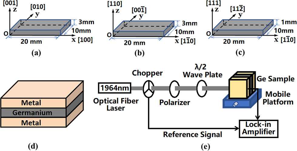
The Ge samples used in the experiments are unintentionally doped N-type Ge single crystals with resistivity of about , and the main impurities are arsenic donors. Based on the resistivity, the impurity concentration is calculated to be about , which is close to the intrinsic carrier concentration of Ge. The sizes of the Ge samples and the experimental system are illustrated in Fig. 1. The shapes of the Ge samples are rectangular parallelepiped, with all six surfaces being mechanically polished before experiments.
Figure 1.Ge samples and the measurement setup of EFI OR. (a) The Ge(001) samples; (b) the Ge(110) samples; (c) the Ge(111) samples; (d) the metal–semiconductor–metal configuration of Ge samples; (e) the measurement system for EFI OR.
The experimental system for testing EFI OR is shown in Fig. 1(e). A continuous wave optical fiber laser with the wavelength of 1964 nm is used, whose power can be adjusted in the range of . The laser output is a Gaussian beam with the waist radius of 1580 μm, which was chopped, the chopper provided a reference signal for the lock-in amplifier, and the voltage signals of EFI OR from the Ge samples were measured by the lock-in amplifier. The polarization direction of the polarizer is along the vertical direction. The azimuth angle of the linearly polarized light can be modified by rotating the half-wave plate.
We investigated the dependence of EFI OR on the polarization direction of the optical wave field. In experiments, we tried to align the laser beam with one of the two depletion regions of the Ge sample, so that we could get the maximum voltage signal of EFI OR. By rotating the half-wave plate to change the azimuth angle of the linearly polarized light, we measured the signals of the EFI OR at the different azimuth angles. The measured anisotropy of the EFI OR was shown in Fig. 2.
Figure 2.EFI OR signals versus the polarization azimuth of the probing beam in the (a) Ge(001), (b) Ge(110), and (c) Ge(111) surface layers.
In the experiments, the laser beam propagates along the axis, so the polarization direction of the optical wave field is in the XOZ plane; then, the optical wave field only has and components, expressed as follows:
Due to the natural interruption of the crystal lattice and the electric field in the depletion layers, the symmetries of the surface layers of Ge(001), Ge(110), and Ge(111) samples should belong to the point groups of , , and . Thus, according to the theory of the second-order nonlinear optics[19], the components of the DC polarization intensity for Ge(001), Ge(110), and Ge(111) samples have the same form and can be deduced as where is the permittivity of Ge, and are components of the effective second-order susceptibility tensor in the surface layers of Ge samples, and is the azimuth of linearly polarized light. According to the Eq. (2), the OR signals should be in a cosine relationship with the angle.
In Fig. 2, the stars represent the experimental data, and the solid lines indicate the fitted curves based on the experimental data, so the equations for the fitted curves for the Ge(001), Ge(110), and Ge(111) surface layers can be written separately as Eqs. (3)–(5): where is the signal of EFI OR, whose unit is microvolts. The experimental data can be fitted with a cosine function with a period of , which is in good accordance with the theoretical Eq. (2). It is proved that there are EFI OR effects in the Ge(001), Ge(110), and Ge(111) surface layers. The operating temperature of the fiber laser is easily affected by the environment condition and the operation time. For example, the temperature of the fiber laser will slowly increase with the operation time, so the laser power will fluctuate slightly, which may induce the deviation of the fitted curve from the experimental data.
According to the corresponding theoretical and experimental relationship based on Eqs. (2) and (3)–(5), the ratios of the two components of effective second-order nonlinear susceptibility tensor in Ge(001), Ge(110), and Ge(111) surface layers can be estimated to be about 0.92, 0.91, and 1.07, respectively. The results show that the magnitudes of two second-order nonlinear susceptibility elements of Ge are close to each other, so the sum of the two components is much larger than their difference. That is why the OR signal has a rather large background in Fig. 2.
In addition, we further investigated the distributions of EFI OR along the normal direction for Ge(001) and Ge(110) crystals, respectively. The laser was fixed in experiments, while an optical displacement platform was used to move the sample along the -axis direction in order to make the laser spot in turn pass through one surface layer of the Ge sample, the sample bulk, the other surface layer of the sample, and finally leave the sample. For decreasing the measurement error, we aligned all of the optical axes of the optical elements with the laser beam in experiments, that is, we let the laser beam irradiate vertically on the input plane of the optical elements and the Ge sample. When laterally moving the Ge sample, we also observed the reflected laser beam from the Ge sample and ensured that the reflected laser beam coincided with the input beam. In order to save the measurement time and avoid fluctuation of laser output power caused by the temperature increase, from the signals appearing until the signal steeply rises, we moved the sample in 50 μm steps; around the peak position, we moved the sample in 20 μm steps. EFI OR signals versus the sample displacement are shown in Fig. 3.
Figure 3.Distribution of the normalized EFI OR signals along the normal direction of the Ge crystal. (a) Along the 001 direction for the Ge(001) samples. (b) Along the 110 direction for the Ge(110) samples.
According to the experimental data fitted method[15], the EFI OR signals are normalized, as shown in Fig. 3. The two surface layers are defined as No. 1 and No. 2, respectively. At the interfaces between Ge and the electrodes, the built-in electric field intensity of the space charge region is the strongest, so the two maximums of EFI OR signals should individually correspond to the overlaps of the Gaussian beam center and the two surfaces. For convenience, the location of the first interface between the metal electrode and Ge, where the EFI OR signal has the first maximum, was defined as the origin of the displacement.
Due to the laser waist radius being 1580 μm, the edge of the laser spot still overlaps with the two depletion layers when the laser beam center moves in the bulk of the Ge sample, so the non-zero EFI OR signals corresponding to the sample bulk region result from the overlap of the distributions of EFI OR in the two surface layers.
The distance between the two surface layers of the Ge(001) crystal shown in Fig. 3(a) is 2920 μm, which is consistent with the thickness of the sample after being polished. The ratio of the OR signal of the No. 1 surface to that of the No. 2 surface is 1:0.933, which indicates that the maximum EFI of the two crystal surface layers is close. In Fig. 3, the solid lines are the theoretically fitted curves to the experimental data, in which the ratio of the two maximum electric field intensities is fixed at 1:0.966; the simulated curve matches the experimental data well. The electric field intensity of the No.1 surface is 1.04 larger than that of the No. 2 surface, indicating that the electric field distributions in two surface layers are very similar. For the experimental results of the Ge(110) crystal, as shown in Fig. 3(b), the simulated curve of the distribution of the normalized OR signals is also in good accordance with the experimental data. These investigated results denote that the EFI OR can be used as an effective method to explore the properties on surface layers of crystals.
In summary, we demonstrated the EFI OR effects in surface layers of Ge(001), Ge(110), and Ge(111) samples under the same experimental conditions and investigated the distributions of the EFI OR signals along the normal directions for the Ge(001) and Ge(110) samples. The change of the OR signals with the azimuth of the polarized probing light exhibits a cosine function of a double azimuth angle, which is consistent with the theoretical expectation. It is proved that there is a significant EFI OR effect in the surface layers of Ge. The ratios of two effective second-order susceptibility tensor elements for the Ge(001), Ge(110), and Ge(111) surface layers were estimated to be about 0.92, 0.91, and 1.07, respectively. In a word, the results indicate that the EFI OR may be as a potential nondestructive method to investigate and compare the surface/interface properties of centrosymmetric crystals and also find potential applications in Ge photonics and optoelectronics.
[14] J. C. Zhu, G. Jia, X. H. Liu, J. B. Sun, Z. P. Zhang, J. X. Zhao, J. B. Mou, Z. G. Chen. Infrared Laser Eng., 40, 1485(2011).
[15] Q. Wang, L. Zhang, X. Wang, H. Y. Quan, Z. G. Chen, J. H. Zhao, X. H. Liu, L. X. Hou, Y. J. Gao, G. Jia, S. W. Chen. Chin. Opt. Lett., 15, 062401(2017).
[16] Q. Wang, H. Zhang, N. Liu, B. J. Zhao, X. H. Liu, L. X. Hou, Y. J. Gao, G. Jia, Z. G. Chen. Chin. Opt. Lett., 14, 012301(2016).