Abstract
For crystals, depressed cladding waveguides have advantages such as preservation of the spectroscopic as well as non-linear properties and the capability to guide both horizontal and vertical polarization modes, but fabrication is always quite time consuming. In addition, it is usually difficult to couple modes propagating in different depressed cladding waveguides through evanescent field overlap, so it is often required to dynamically reconfigure photonic waveguide devices using external fields for classical or quantum applications. Here, we experimentally demonstrate the single-scan femtosecond laser transverse writing of depressed cladding waveguides to form a directional coupler inside lithium niobate crystal, which is integrated with two deeply embedded microelectrodes on both sides of the interaction region to reconfigure the coupling. By focal field engineering of the femtosecond laser, we specially generate a three-dimensional longitudinally oriented ring-shaped focal intensity profile composed of 16 discrete spots to simultaneously write the entire cladding region. The fabricated waveguides exhibit good single guided modes in two orthogonal polarizations at 1550 nm. By applying voltage to the deeply embedded microelectrodes fabricated with the femtosecond laser ablation followed by selective electroless plating, we successfully facilitate the light coupling from the input arm to the cross arm and thus actively tune the splitting ratio. These results open new important perspectives in the efficient fabrication of reconfigurable complex three-dimensional devices in crystals based on depressed cladding waveguides.1. INTRODUCTION
Femtosecond laser inscription, serving as a versatile tool for various transparent material processing [1–4], has been used to fabricate devices based on optical waveguides, such as beam splitters [5] and Mach–Zehnder interferometers [6]. Particularly, it has the ability to build true three-dimensional (3D) microstructures and to construct 3D photonic circuits [7], without the need for masking and etching steps commonly associated with photolithography [8,9]. The directional coupler (DC) is the integrated optical analogue to a bulk beam splitter and thus is the fundamental building block of classical and quantum optical circuits [10]. Geometrically, a DC consists of two identical waveguides as two arms, which are brought together with a close center-to-center interaction distance for a certain interaction length. It has often been realized in glasses based on type I waveguides whose guiding cores are formed directly at the focal volume leading to the change of original properties of the bulk materials [1]. Nevertheless, different from the amorphous structure of glasses, the large natural positional order of the lattices in the crystalline structure makes it difficult to achieve a refractive index increase induced by the material densification. The refractive index changes depend on both the laser beam parameters and crystal lattice structures [11]. Moreover, preservation of the spectroscopic and nonlinear properties in the waveguide core is extremely important for crystals, so that stress-induced waveguides and depressed cladding waveguides have been developed. They comprise severe damage tracks with a negative refractive index change produced in the crystal at higher pulse energies [12–14].
Although the simple “dual-line” stress-induced waveguides can guide both the horizontal (H) and vertical (V) polarization modes in some vanadate crystals, they support only one polarization mode in Nd:YAG and lithium niobate crystal () [15]. Depressed cladding waveguides with more flexible shape and core size may confine both H and V polarizations with low polarization dependence in most crystals. However, it is considerably difficult to fabricate a DC on the basis of depressed cladding waveguides for two main reasons. On the one hand, femtosecond laser transverse writing of a single depressed cladding waveguide is quite time-consuming and hard to control, since many depressed tracks in different depths are inscribed one by one using the original ellipsoidal focal spot of the laser, let alone fabricating a more complex circuit composed of several depressed cladding waveguides. In 2016, Qi et al. effectively reduced the scan times to only four for fabricating a square-shaped depressed cladding waveguide using a line-shaped beam [16] generated by slits at the expense of heavy energy losses. Compared with square-shaped claddings, circular-shaped claddings are better to keep the modal profiles along a complex photonic circuit and are more convenient in terms of coupling with external elements such as single-mode fibers (SMFs). More recently, we have developed a single-scan scheme for simultaneous modification of the entire region of the depressed cladding at the cross section in ZBLAN glasses [17].
Nevertheless, it is not straightforward to extend this single-scan scheme to crystals due to the complexity of crystalline structures, bulk chemical/physical features, high birefringence, and large spherical aberration introduced by focusing the incident laser beam through an interface between air and the high-refractive-index crystal. On the other hand, it is pretty difficult to couple two modes propagating in two arms of a DC through evanescent field overlap because severely modified depressed claddings hinder efficient light field exchange unless substantially extending the interaction length, which is in turn unfavorable for integration. At the same time, it is usually tough to determine the right length to obtain the desired splitting ratio. It gets even harder to simultaneously guarantee the accuracy of each DC when combining several DCs with different splitting ratios together to build a complex circuit because fabrication errors are inevitable and need compensation. Furthermore, the functionalities, i.e., the splitting ratios, of the circuit sometimes need dynamic changes according to different implementations [18], so the reconfigurability of the elements is in demand. Electro-optic tuning is considered a convenient choice because of its simplicity and stability. is very attractive for its large nonlinear optical as well as electro-optic coefficients and has been fully exploited for many active devices serving for both classical and quantum photonic applications [19–21]. Integrating electrodes into waveguides circuits has been realized commonly through planar lithographic methods [22], which is limited in producing deeply embedded 3D electrodes with improved electro-optic interaction for waveguides buried inside crystal rather than on the surface.
Sign up for Photonics Research TOC. Get the latest issue of Photonics Research delivered right to you!Sign up now
In this work, we report the fabrication of a reconfigurable DC composed of two identical single-scan depressed cladding waveguides integrated with two deeply embedded microelectrodes on both sides of the interaction region inside crystal, as illustrated in Fig. 1. An engineered femtosecond laser with a longitudinally oriented discrete ring-shaped focal intensity profile, generated by loading a specially designed phase mask onto a spatial light modulator (SLM), is used to transversely inscribe the depressed cladding waveguide in a single-scan scheme. The fabricated waveguide exhibits good single guided modes for both H and V polarizations at 1550 nm. To realize the reconfigurability of the DC, femtosecond laser ablation with subsequent femtosecond-laser-assisted selective electroless plating is used to fabricate embedded electrodes with a depth of . Hence, waveguides are located in the middle of the electrodes in the axis. By applying voltage to the electrodes, facilitated light coupling from one arm to the other and tunable splitting ratio are successfully demonstrated. These results embody significant benefits for efficient and reconfigurable complex 3D photonic circuits consisting of depressed cladding waveguides in crystal.
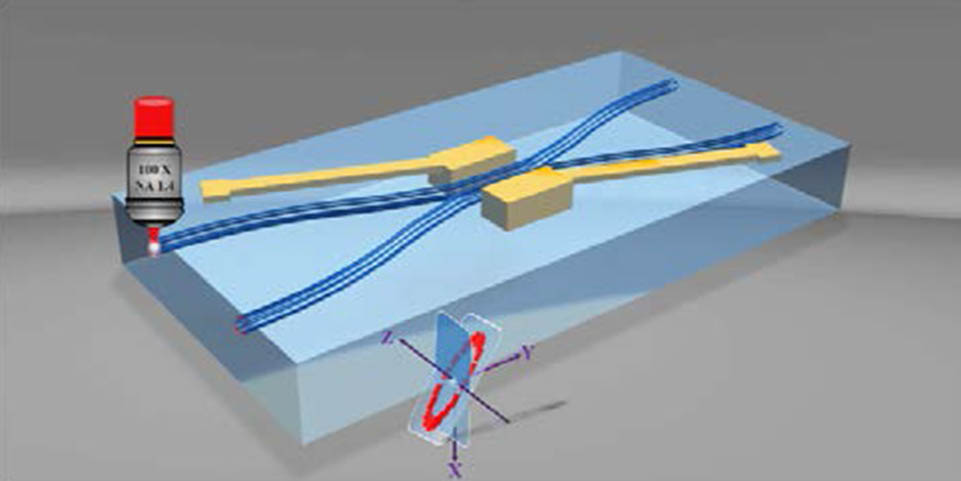
Figure 1.Schematic for transverse writing of reconfigurable DC based on depressed cladding waveguides. Circular cladding composed of dozens of parallel filaments formed through single scan using a longitudinal discrete ring-shaped focal intensity profile. The ring is tilted 10° with respect to axis.
2. FOCAL FIELD ENGINEERING
To generate the longitudinal discrete ring-shaped focal intensity distribution oriented along the laser propagation direction, we use the weighted Yang-Gu algorithm [23] to design the phase mask, as described in detail in our previous work [17]. The convergence time is shortened to only four hours under parallel calculation with a workstation (HP Z840). We also halve the sampling interval in the – plane as well as double the -slice number compared with those in Ref. [15]. Experimental results indicate that femtosecond laser pulses prefer to produce discrete depressed index structures inside instead of continuous ones [17]. Hence, the designed targeted focal intensity profile consists of 16 discrete spots arranged in a circle, as shown in Fig. 2(a). Different circle diameters lead to different mode field diameters (MFDs). To well match the MFD of the SMF at 1550 nm, we select a diameter of according to experimental results. Each spot is generated using the vectorial Debye integral, which is suitable to calculate the diffraction field in the focal region of an objective with high numerical aperture [24]. One big problem is the severe interference among spots when placing them together to form the ring, which leads to undesired extra intensity distribution both inside and outside the ring and non-uniform intensity of the spots themselves. So we specially adjust the incident amplitude for generating each spot to make the whole ring more uniform. The intensity ring is tilted 10° with respect to the axis, to prevent perturbation of the beam passing through the previously modified areas. The calculated phase mask is presented in Fig. 2(b). The simulated 3D isosurface (the isosurface is given by the intensity at 45% of the peak value) intensity profile is shown in Fig. 2(c). It can be seen that the simulated profile follows the designed target [Fig. 2(a)] pretty well.

Figure 2.(a) 3D isosurface of the targeted 3D focal intensity profile (the isosurface is given by the intensity at 45% of the peak value). (b) Calculated phase mask. (c) Corresponding simulated 3D isosurface intensity profile. The sample is translated along axis.
However, not all the spots have the same size, which means that smaller spots require higher pulse energy than bigger ones in the fabrication. This slight non-uniformity might be caused by slight interaction between neighboring spots and the non-uniformity of the generated target itself [Fig. 2(a)]. Fortunately, experimental results show that it does not affect the overall morphology of the cladding.
3. EXPERIMENT
A commercially available MgO-doped -cut crystal of a size of with four optically polished surfaces is used in our experiment. The experimental setup is almost the same as that in Ref. [15]. Waveguides are inscribed by a regeneratively amplified Yb:KGW system (Pharos-20 W–1 MHz, Light Conversion) producing pulses at 1030 nm at a repetition rate of 200 kHz. The incident laser beam is modulated by a reflective phase-only SLM (X13138-03, Hamamatsu). The engineered beam is then imaged onto the back aperture of an oil immersion objective lens (UPLAN, , Olympus) and focused into the crystal sample to inscribe waveguides. The non-fluorescent immersion oil (refractive index , Olympus) is used during the fabrication, so the spherical aberration, caused by refractive indices mismatch in the interface, is mitigated. The residual spherical aberration appropriately elongates the spots along the axis to write the cladding with a thicker thickness, which is good for reducing losses [25]. We fabricate 10-mm-long straight waveguides at a depth of with a pulse energy of 1.55 μJ. The sample is translated along the axis in the same direction as the laser polarization at 1 mm/s by a computer-controlled high-precision, three-axis air-bearing stage (FG1000-150-5-25-LN, Aerotech). Figures 3(a) and 3(b) show the cross section and the top view of the waveguide, respectively. Compared with Fig. 2(c), the inscribed tracks are elongated along the axis [see Fig. 3(a)] primarily due to the effect of spherical aberration and thus serve well as the cladding with a thickness of , which is enough to confine light. Deeper waveguides may need additional correction to the phase masks to counterbalance more evident spherical aberration effects [26]. The fabricated cladding is indeed a discrete annular ring according to our design with a relatively uniform intensity profile and without extra tracks. The waveguide is really smooth without a trace of microexplosion, which might be induced by laser irradiation.
Figure 3.Optical micrographs and guided modes of a waveguide written through the discrete ring-shaped focal field. (a) Cross section of the depressed cladding. (b) Top view of the waveguide. (c), (d) 2D intensity distribution images of the guided H and V polarization modes at 1550 nm, respectively.
We input a CW laser (SIFC, Thorlabs) with a wavelength of 1550 nm through an SMF, which is butt-coupled to the waveguide without refractive-index-matching oil. At the same time, we use an InGaAs camera (C12741-03-01, Hamamatsu), combined with a microscope objective (), to image near-field mode profiles at the exit facet of the waveguide. It can be clearly seen that the depressed cladding waveguide can guide both H and V polarization modes, as presented in Figs. 3(c) and 3(d), respectively. The mode field areas are for H mode and for V mode. The values are very close to the MFD of the SMF at 1550 nm, i.e., , so the coupling loss is pretty low, which is estimated to be 0.07 dB/facet for H mode and 0.08 dB/facet for V mode via numerically evaluating the mode overlapping integral [27]. By measuring the input power of the laser and the output power from the waveguide, the insertion loss is estimated to be 2.95 dB for H mode and 1.63 dB for V mode. The propagation loss can be obtained by subtracting the coupling losses and Fresnel reflection losses from the insertion loss, which is estimated to be 2.58 dB/cm for H mode and 1.25 dB/cm for V mode. By measuring the cone angle of the emerging light [28], the measured refractive index change is . These results demonstrate nearly polarization-independent guiding behavior, which might be owed to more isotropic stress distribution, as the refractive index change takes place almost only in the depressed cladding compared with the “double-line” structures in which not only a negative refractive index change arises in the two laser-written lines, but also a stress-induced positive refractive index change appears between the double lines [29].
We further fabricate a DC with an interaction distance of (the width of each waveguide is ) and an interaction length of . For the curved segments, a 60 mm bending radius is adopted, which gives of additional bending losses on the whole device. Figure 4(a) shows top views of the straight interaction region (middle) and two curved segments (left and right) of the DC without the integrated electrodes. The fabrication procedure of the embedded 3D electrodes consists mainly of three steps, including water-assisted femtosecond laser ablation of vertical microgrooves, formation of catalyst films inside the ablated grooves, and electroless copper plating. Details of the fabrication process can be found elsewhere [30–32]. The fabricated electrodes and their connecting lines as well as pads are presented in Fig. 4(b). The shape of the electrodes is finely controlled to a cuboid with vertical inner surfaces according to our design, and the copper is almost fully filled inside such deep grooves (). Using the matrix-ablation technique, the shape and dimension of the electrodes and thus the electric field can be accurately controlled by changing the parameters of the femtosecond laser ablation. We numerically simulate the electric field inside the sample using finite-element method [33], as shown in Fig. 4(c). The result shows that the electric field across the waveguides is very uniform and well confined along the axis with the largest electro-optic coefficient.
Figure 4.Optical micrographs; numerical simulation of the electric field between the two electrodes and guided mode of a DC written by using the discrete ring-shaped focal field. (a) Top views of the straight interaction region (middle) and two curved segments (left and right) of the DC without the integrated electrodes. (b) Top view of the electrodes and their connecting lines. Inset: connecting line with a pad at the end. (c) Equipotential contour of the electric field around the electrodes. (d) Splitting ratio with the increase in applied voltage to the electrode. (e) Output intensity of the DC for the guided V mode at 1550 nm with three voltages.
To characterize the device, we input a -polarized laser to one input port of the DC and use a pair of probe needles connected with an external electric source to apply voltage to the two metallic pads at the end of the connecting lines starting from the two electrodes (see Fig. 1). At the same time, we record the change of the splitting ratio (ratio of the output powers from the cross arm and the input arm) with the applied voltage. The initial transmitted power in the output cross arm is due to the short interaction length. We gradually increase the applied voltage and observe facilitated light coupling from the input arm to the cross arm from . The splitting ratio becomes higher and higher in the process of the voltage increasing, as shown in Fig. 4(d). The guided modes with different applied voltages are shown in Fig. 4(e). We foresee that achieving nearly total transmission from initial total reflection status needs very high applied voltage [34]. This may be because the depressed waveguide is much wider than a type I waveguide, so it is inherently more difficult to change the refractive index near the cladding region. Moreover, the refractive index of the material surrounding two closely adjacent depressed waveguides needs adjusting at the same time, which further expands the targeted region. Therefore, very high applied voltage could bring a remarkable refractive index change as well as splitting ratio change. Since the gap between the two electrodes is relatively small (), we cannot apply too much voltage in case of damaging the crystal. In the future, we can extend the dimension of the electrodes or add extra electrodes between the two arms to improve the amplitude and efficiency of the electro-optic modulation and thus improve the reconfigurability of the coupler device. We also measure the splitting ratio change for H polarization within the same range of applied voltages (0–600 V). As expected, it is almost the same because the guidance of the waveguides is nearly polarization independent as described above.
4. CONCLUSION
In conclusion, we have demonstrated the femtosecond laser transverse inscription of a reconfigurable DC inside crystal based on efficient single-scan depressed cladding waveguides using the specially designed longitudinally oriented discrete ring-shaped focal field of the laser. The entire region of the depressed cladding composed of 16 parallel damage tracks at the cross section is modified simultaneously through a single scan. The deeply embedded 3D electrodes are fabricated using femtosecond laser ablation subsequently with femtosecond-laser-assisted selective electroless plating. The shape of the electrodes is finely controlled to a cuboid with vertical inner surfaces according to our design, and the copper is almost fully filled inside the ablated deep grooves. The waveguides exhibit good single guided modes in both H and V polarizations at a wavelength of 1550 nm. By gradually increasing the voltage applied to the electrodes, we can clearly see the increase in the splitting ratio of the DC. The amplitude of the electro-optic modulation can be improved by finely designing the geometry of electrodes as well as DC and by increasing the number of electrodes in the future. These results open new important perspectives in the efficient fabrication of complex 3D devices in crystals based on depressed cladding waveguides.
References
[1] R. R. Gattass, E. Mazur. Femtosecond laser micromachining in transparent materials. Nat. Photonics, 2, 219-225(2008).
[2] A. M. Streltsov, N. F. Borrelli. Fabrication and analysis of a directional coupler written in glass by nanojoule femtosecond laser pulses. Opt. Lett., 26, 42-43(2001).
[3] S. Maruo, J. T. Fourkas. Recent progress in multiphoton microfabrication. Laser Photon. Rev., 2, 100-111(2008).
[4] K. M. Davis, K. Miura, N. Sugimoto, K. Hirao. Writing waveguides in glass with a femtosecond laser. Opt. Lett., 21, 1729-1731(1996).
[5] S. Nolte, M. Will, J. Burghoff, A. Tuennermann. Femtosecond waveguide writing: a new avenue to three-dimensional integrated optics. Appl. Phys. A, 77, 109-111(2003).
[6] A. Crespi, Y. Gu, B. Ngamsom, H. J. W. M. Hoekstra, C. Dongre, M. Pollnau, R. Ramponi, H. H. V. D. Vlekkert, P. Watts, G. Cerullo, R. Osellame. Three-dimensional Mach-Zehnder interferometer in a microfluidic chip for spatially-resolved label-free detection. Lab Chip, 10, 1167-1173(2010).
[7] Y. Zhang, Q. Chen, H. Xia, H. Sun. Designable 3D nanofabrication by femtosecond laser direct writing. Nano Today, 5, 435-448(2010).
[8] G. A. Shafeev. Laser activation and metallisation of insulators. Quantum Electron., 27, 1104-1110(1997).
[9] M. D. Levenson, N. S. Viswanathan, R. A. Simpson. Improving resolution in photolithography with a phase-shifting mask. IEEE Trans. Electron. Devices, 29, 1828-1836(1982).
[10] A. Crespi, R. Ramponi, R. Osellame, L. Sansoni, I. Bongioanni, F. Sciarrino, G. Vallone, P. Mataloni. Integrated photonic quantum gates for polarization qubits. Nat. Commun., 2, 566(2011).
[11] F. Chen, J. R. Vazquez de Aldana. Optical waveguides in crystalline dielectric materials produced by femtosecond-laser micromachining. Laser Photon. Rev., 8, 251-275(2014).
[12] R. He, Q. An, Y. Jia, G. R. Castillo-Vega, J. R. V. Aldana, F. Chen. Femtosecond laser micromachining of lithium niobate depressed cladding waveguides. Opt. Mater. Express, 3, 1378-1384(2013).
[13] A. G. Okhrimchuk, A. V. Shestakov, I. Khrushchev, J. Mitchell. Depressed cladding, buried waveguide laser formed in a YAG: Nd3+ crystal by femtosecond laser writing. Opt. Lett., 30, 2248-2250(2005).
[14] H. D. Nguyen, A. Ródenas, J. R. V. Aldana, G. Martín, J. Martínez, M. Aguiló, M. C. Pujol, F. Díaz. Low-loss 3D-laser-written mid-infrared LiNbO3 depressed-index cladding waveguides for both TE and TM polarizations. Opt. Express, 25, 3722-3736(2017).
[15] Y. Tan, A. Rodenas, F. Chen, R. R. Thomson, A. K. Kar, D. Jaque, Q. Lu. 70% slope efficiency from an ultrafast laser-written Nd:GdVO4 channel waveguide laser. Opt. Express, 18, 24994-24999(2010).
[16] J. Qi, P. Wang, Y. Liao, W. Chu, Z. Liu, Z. Wang, L. Qiao, Y. Cheng. Fabrication of polarization-independent single-mode waveguides in lithium niobate crystal with femtosecond laser pulses. Opt. Mater. Express, 6, 2554-2559(2016).
[17] Q. Zhang, D. Yang, J. Qi, Y. Cheng, Q. Gong, Y. Li. Single scan femtosecond laser transverse writing of depressed cladding waveguides enabled by three-dimensional focal field engineering. Opt. Express, 25, 13263-13270(2017).
[18] F. Flamini, L. Magrini, A. S. Rab, N. Spagnolo, V. D’Ambrosio, P. Mataloni, F. Sciarrino, T. Zandrini, A. Crespi, R. Ramponi, R. Osellame. Thermally reconfigurable quantum photonic circuits at telecom wavelength by femtosecond laser micromachining. Light Sci. Appl., 4, e354(2015).
[19] Y. Liao, J. Xu, Y. Cheng, Z. Zhou, F. He, H. Sun, J. Song, X. Wang, Z. Xu, K. Sugioka, K. Midorikawa. Electro-optic integration of embedded electrodes and waveguides in LiNbO3 using a femtosecond laser. Opt. Lett., 33, 2281-2283(2008).
[20] M. Papuchon, Y. Combemale, X. Mathieu, D. B. Ostrowsky, L. Reiber, A. M. Roy, B. Sejourne, M. Werner. Electrically switched optical directional coupler: cobra. Appl. Phys. Lett., 27, 289-291(1975).
[21] G. K. Gopalakrishnan, C. H. Bulmer, W. K. Burns, R. W. McElhanon, A. S. Greenblatt. 40 GHz, low half-wave voltage Ti:LiNbO3, intensity modulator. Electron. Lett., 28, 826-827(1992).
[22] E. L. Wooten, K. M. Kissa, A. Yi-Yan, E. J. Murphy, D. A. Lafaw, P. F. Hallemeier, D. Maack, D. V. Attanasio, D. J. Fritz, G. J. McBrien, D. E. Bossi. A review of lithium niobate modulators for fiber-optic communications systems. IEEE J. Sel. Top. Quantum Electron., 6, 69-82(2000).
[23] X. Yu, K. Chen, Y. Zhang. Optimization design of diffractive phase elements for beam shaping. Appl. Opt., 50, 5938-5943(2011).
[24] P. Török, P. Varga, Z. Laczik, G. R. Booker. Electromagnetic diffraction of light focused through a planar interface between materials of mismatched refractive indices: an integral representation. J. Opt. Soc. Am. A, 12, 325-332(1995).
[25] D. G. Lancaster, S. Gross, H. Ebendorff-Heidepriem, K. Kuan, T. M. Monro, M. Ams, A. Fuerbach, M. J. Withford. Fifty percent internal slope efficiency femtosecond direct-written Tm3+ ZBLAN waveguide laser. Opt. Lett., 36, 1587-1589(2011).
[26] L. Huang, P. S. Salter, F. Payne, M. J. Booth. Aberration correction for direct laser written waveguides in a transverse geometry. Opt. Express, 24, 10565-10574(2016).
[27] R. Zhang, J. Wang, G. Zhao, J. Lv. Fiber-based free-space optical coherent receiver with vibration compensation mechanism. Opt. Express, 21, 18434-18441(2013).
[28] J. A. Dharmadhikari, A. K. Dharmadhikari, A. Bhatnagar, A. Mallik, P. C. Singh, R. K. Dhaman, K. Chalapathi, D. Mathur. Writing low-loss waveguides in borosilicate (BK7) glass with a low-repetition-rate femtosecond laser. Opt. Commun., 284, 630-634(2011).
[29] J. Burghoff, S. Nolte, A. Tünnermann. Origins of waveguiding in femtosecond laser-structured LiNbO3. Appl. Phys. A, 89, 127-132(2007).
[30] J. Xu, Y. Liao, H. Zeng, Z. Zhou, H. Sun, J. Song, X. Wang, Y. Cheng, Z. Xu, K. Sugioka, K. Midorikawa. Selective metallization on insulator surfaces with femtosecond laser pulses. Opt. Express, 15, 12743-12748(2007).
[31] Y. Liao, J. Xu, H. Sun, J. Song, X. Wang, Y. Cheng. Fabrication of microelectrodes deeply embedded in LiNbO3 using a femtosecond laser. Appl. Surf. Sci., 254, 7018-7021(2008).
[32] J. Xu, D. Wu, J. Y. Ip, K. Midorikawa, K. Sugioka. Vertical sidewall electrodes monolithically integrated into 3D glass microfluidic chips using water-assisted femtosecond-laser fabrication for in situ control of electrotaxis. RSC Adv., 5, 24072-24080(2015).
[33] L. N. Binh. Lithium niobate optical modulators: devices and applications. J. Cryst. Growth, 288, 180-187(2006).
[34] S. Kroesen, W. Horn, J. Imbrock, C. Denz. Electro-optical tunable waveguide embedded multiscan Bragg gratings in lithium niobate by direct femtosecond laser writing. Opt. Express, 22, 23339-23348(2014).


