• Acta Photonica Sinica
  • Vol. 51, Issue 2, 0251208 (2022)
Chao NING1、2, Ruixuan SUN1、2, Tian YU1、2, Shuman LIU1、2、*, Jinchuan ZHANG1、2, Ning ZHUO1、2, Lijun WANG1、2, Junqi LIU1、2, Shenqiang ZHAI1、2, Yuan LI1, and Fengqi LIU1、2、3
Author Affiliations
  • 1Key Laboratory of Semiconductor Materials Science,Institute of Semiconductors,Chinese Academy of Sciences,Beijing 100083,China
  • 2Center of Materials Science and Opto-electronic Engineering,University of Chinese Academy of Sciences,Beijing 100049,China
  • 3Beijing Academy of Quantum Information Sciences,Beijing 100193,China
  • show less
    DOI: 10.3788/gzxb20225102.0251208 Cite this Article
    Chao NING, Ruixuan SUN, Tian YU, Shuman LIU, Jinchuan ZHANG, Ning ZHUO, Lijun WANG, Junqi LIU, Shenqiang ZHAI, Yuan LI, Fengqi LIU. Optimization of Electron Injectors for Interband Cascade Lasers(Invited)[J]. Acta Photonica Sinica, 2022, 51(2): 0251208 Copy Citation Text show less

    Abstract

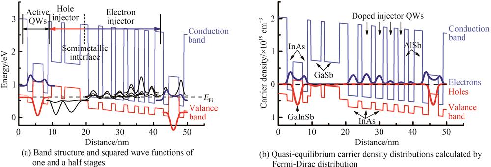
    The Interband Cascade Laser (ICL) is a mid-infrared laser source with a low threshold current density, which has been used widely in hydrocarbon detection and other gases. One active region stage of an ICL consists of an InAs/GaInSb/InAs W Quantum Well (QW) emitter, GaSb/AlSb QW hole injector and InAs/AlSb chirped superlattice electron injector. In contrast to the intersubband electron transition and transportation in quantum cascade lasers, interband transitions and carrier transportation from valance band to conduction band through a semimetallic interface are involved in an ICL. As the electron injector is longer than the hole injector, most ionized electrons are located in the lower subbands away from the emitter, and the efficiency of electron injection into the emitter is lower than that of holes, resulting in a large number of excess holes in the emitter. The existence of these holes causes the non-radiative Auger recombination and deteriorates the laser performance. Heavy doping, on the other size, may cause large free-carrier absorption loss and impurity scattering loss in the active region. In this work, the thickness of the electron injector was thinned to improve the electron injection efficiency by increasing the subband energy level of the electron injector. The doping concentration required for the carriers’ rebalance was reduced, which led to a low internal loss.Two ICL wafers were grown in a molecular beam epitaxy system on Te-doped GaSb substrates. achieved excellent room temperature lasing performance. One stage of the active region of sample S1 is as follows: 2.5 nm AlSb/1.8 nm InAs/3.0 nm Ga0.7In0.3Sb/1.5 nm InAs/1.0 nm AlSb/3.0 nm GaSb/1.0 nm AlSb/4.5 nm GaSb/2.0 nm AlSb/3.4 nm InAs/1.2 nm AlSb/3.0 nm InAs/1.2 nm AlSb/2.6 nm InAs/1.2 nm AlSb/2.1 nm InAs/1.2 nm AlSb/1.8 nm InAs/1.2 nm AlSb/1.8 nm InAs, where the underlined InAs QWs were doped with Si to 2×1018 cm3. For comparison, sample S2 with a thick electron injector of 4.2 nm InAs/1.2 nm AlSb/3.2 nm InAs/1.2 nm AlSb/2.5 nm InAs/1.2 nm AlSb/2.1 nm InAs/1.2 nm AlSb/1.8 nm InAs/1.2 nm AlSb/1.8 nm InAs and a Ga0.65In0.35Sb hole QW in the emitter was grown. The electron subband of the thick electron injector in sample S2 is lower than that in sample S1, resulting in an inefficient electron injection into the emitter.Laser bars with a 4-mm-long cavity and 20-μm-wide ridge were fabricated from wafers S1 and S2. They exhibit similar threshold current of 200 mA and output power of 55 mW per facet, while sample S1 shows a turn-on voltage 2.3 V high than sample S2. The calculated energy band structures of the two samples indicate that the semimetallic interface for resonant tunneling in sample S1 is formed at a high electric field of 170 kV compared to 85 kV for sample S2, which is agreed to the high turn-on voltage of sample 1. Furthermore, the variable cavity length analysis on a series of laser bars with different cavity lengths was conducted to extract the waveguide loss αw, internal quantum efficiency ηi, differential current gain G, transparency current density Jtr, and carrier lifetime τ for the two samples. As expected, sample S1 with a thin electron injector has a waveguide loss of 3 cm-1, which is lower than 4.79 cm-1 for sample S2 with a thick electron injector. Other extracted parameters are similar for the two wafers, including the carrier lifetime of 0.7 ns. Theoretically, sample S1 with lower waveguide loss should have a long carrier lifetime. It is noted that the strain of GaInSb QWs relative to GaSb substrates is larger for sample S2. It is known that a large strain results in a strong decoupling of the heavy-hole and light-hole subband edge, which is beneficial to suppress the PPN auger nonradiative recombination in the emitter. Thus the large strain in sample S2 tends to compensate to a certain extent the effect of carrier injection unbalance on the gain of the emitter. The combined effect is that the carrier lifetimes of the two samples are almost same.In summary, the reduced InAs QWs thicknesses of the electron injector in the ICL designed in this work improved the electron injection efficiency, thereby balancing the carrier density with low doping concentration. The laser with lowered doping concentration and thin electron injectors produced a waveguide loss as low as 3 cm-1. The laser performance is expected to be improved by increasing the strain to reduce the Auger recombination further.
    Chao NING, Ruixuan SUN, Tian YU, Shuman LIU, Jinchuan ZHANG, Ning ZHUO, Lijun WANG, Junqi LIU, Shenqiang ZHAI, Yuan LI, Fengqi LIU. Optimization of Electron Injectors for Interband Cascade Lasers(Invited)[J]. Acta Photonica Sinica, 2022, 51(2): 0251208
    Download Citation