1Key Laboratory of Space Applied Physics and Chemistry, Ministry of Education, and Shaanxi Key Laboratory of Optical Information Technology, School of Science, North Western Polytechnical University, Xi’an 710072, China
2Department of Electrical and Computer Engineering, National University of Singapore, Singapore 117583, Singapore
3LEES Program, Singapore-MIT Alliance for Research & Technology (SMART), Singapore 138602, Singapore
Zhiqiang Yang, Kang Du, Wending Zhang, Soojin Chua, Ting Mei. A polarization-insensitive fishnet/spacer/mirror plasmonic absorber for hot electron photodetection application[J]. Chinese Optics Letters, 2020, 18(5): 052402
Copy Citation Text
A polarization-insensitive plasmonic absorber is designed consisting of Au fishnet structures on a TiO2 spacer/Ag mirror. The fishnet structures excite localized surface plasmon and generate hot electrons from the absorbed photons, while the TiO2 layer induces Fabry–Perot resonance, and the Ag mirror acts as a back reflector. Through optimizing the TiO2 layer thickness, numerical simulation shows that 97% of the incident light is absorbed in the Au layer. The maximum responsivity and external quantum efficiency of the device can approach 5 mA/W and ~1%, respectively, at the wavelength of 700 nm.
Internal photoemission (IPE) occurs inherently in Schottky diodes at the metal-semiconductor interface[1] for hot electrons excitation by light with photon energy greater than the Schottky barrier height[2]. The barrier height is typically lower in energy than the semiconductor bandgap energy[3]. In recent years, due to advancement in manufacturing nanoplasmonic semiconductor devices[4] and Schottky diodes with excellent performance[5], as well as potential applications in solar cells[6,7] and optical communication devices[8,9], the hot electron phenomenon has attracted enthusiastic research attention[10–12] to extend the wavelength range of interest for light harvesting and signal detection.
is a low-cost and widely used optoelectronic material[13]. However, due to its large bandgap of 3.2 eV, it cannot be used for photoelectric conversion in the visible or near-infrared band[14]. A number of recent reports have therefore been directed towards addressing the issue of extending the light harvesting range of to sub-bandgap photon energies[15–17]. In this regard, plasmon-enhanced IPE from metal nanostructures can be applied to these wide bandgap semiconductors, offering an interesting avenue toward the development of novel solar energy harvesting devices[18]. Our previous devices based on the silicon oxide nanocones template were able to achieve photoelectric conversion in the 450–1000 nm wavelength range[19].
Efficiency of IPE could be enhanced by combining a plasmonic absorber[20] with a Schottky diode[21,22]. Li et al.[23] proposed a design of a Schottky-junction hot electron photodetector, in which both the optical Tamm state and Fabry–Perot cavity mode can be excited, leading to an enhancement in the photo responsivity. Fang et al.[24] investigated an electrochemical cell containing an Au-nanodisk antenna/ spacer/Au mirror (ASM) structure using the interaction of the Fabry–Perot resonance (FPR) and localized surface plasmons to strongly enhance photon-to-electron conversion. For solid-state hot electron device application, the ASM structure cannot be directly employed due to lack of electrical connection among the antennas, and it is necessary to investigate a new design of an electrically contacted plasmonic absorber[25]. Moreover, realizing localized surface plasmon resonance (LSPR) and its interplay with FPR can be explored for performance enhancement.
Sign up for Chinese Optics Letters TOC. Get the latest issue of Chinese Optics Letters delivered right to you!Sign up now
In this Letter, we propose an Au-fishnet/ spacer/Ag mirror (FSM) plasmonic absorber, allowing plasmonic resonance for sub-bandgap photon-to-electron conversion in solid-state devices. The Au fishnet and the Ag mirror form a Fabry–Perot cavity with a spacer sandwiched in between. The LSPR can be achieved by tuning the width of lines in the fishnet while keeping the period constant, and its coupling with FPR can be realized by varying the thickness of the . The absorption is concentrated at the top Au fishnet layer, which is desirable for hot electrons to travel cross the Schottky barrier. The theoretical external quantum efficiency (EQE) of this structure is found to reach ∼1%, which exceeds the efficiency reported in Refs. [24,26].
The model for analysis consists of a one-dimensional grating structure consisting of a spacer/Ag mirror structure, as shown in Fig. 1(a). In this structure, the Au grating film is 10 nm thick on the top of a 200 nm thick layer which is on an Ag metal layer. The Ag layer is chosen to be thick enough so that the Ag layer acts as a good reflector. Due to the presence of plasmonic resonance in the metal-dielectric sub-wavelength structure, higher absorption is achieved at some specific wavelengths. Optical and electrical models were developed to analyze the structure under the condition of top illumination. The electric field and hot electron generation rate profile were simulated by using the finite difference time domain method (FDTD Solutions, Lumerical Inc., Canada). The dielectric functions of Au, Ag, and were adopted from Palik[27]. The complete periodic boundary condition was adopted in the and directions, while a perfect match layer was adopted in the direction.
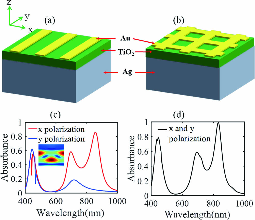
Figure 1.(a) Schematic diagram of Au grating/ spacer/Ag mirror structure; (b) schematic diagram of FSM structure; (c), (d) absorption spectrum under different light polarization conditions corresponding to the structures in (a), (b), respectively. The inset in (c) shows the magnetic field distribution under guided mode resonance conditions at .
Figure 1(c) shows the absorption spectrum corresponding to Fig. 1(a). The grating has each line at a width of 60 nm and a period of 200 nm. The absorption spectrum of the grating structure has obvious polarization dependence, and the resonance peaks at 450 nm and 694 nm exist simultaneously under the incident light in both polarizations. But, as the polarization direction changes from to , the absorption peak at 850 nm disappears completely. This is because the plasmon resonance is excited by the Au grating under polarization and cannot be excited under polarization.
The absorption spectrum also shows sharp absorption valleys at the wavelength of 442 nm and 466 nm when the -polarized and -polarized lights are incident, respectively, on the grating. This is because at these two wavelengths, the conditions for guided mode are met[28], negating the FPR condition and causing a drastic drop in absorption. The magnetic field distribution of the guided mode is shown by the inset in Fig. 1(c).
Figure 1(b) shows the light absorber with the FSM structure, in which identical structural parameters were assigned in the and directions in order to obtain polarization-insensitive response. The Au thickness , thickness , and period are also 10 nm, 200 nm, and 200 nm, respectively. Surface plasmon resonance modes can be excited in both and directions simultaneously. Compared with the absorption spectrum of the grating structure, the absorption of the FSM structure is enhanced at the three peak positions. At 830 nm, the absorption in both polarizations can reach more than 97%. This means that the absorption mechanism of the FSM structure is similar to that of the grating structure under polarization. The drastic changes in the absorption spectrum at the wavelengths of 434 nm and 462 nm indicate that the guided mode resonances of the two polarizations in the grating structure appear simultaneously in the FSM structure.
The optical tunability of the plasmonic structure is illustrated in Fig. 2, where the absorption in the structure is mapped versus wavelength and line width of the fishnet structure with a setting of and for various thicknesses of the film. Large absorption is in red, while blue indicates low absorption. These maps consistently show a number of absorption peak lines denoting different resonance modes. The vertical absorption peak lines shown in these maps do not shift in wavelength when the width of the lines in the fishnet increases, but, with the increase in thickness of the , the absorption peaks gradually red shift.
Figure 2.Absorption in the FSM structure as a function of wavelength and width of the lines in the fishnet for the different thicknesses h of (a) 180 nm, (b) 200 nm, and (c) 220 nm, with and .
These resonances are identified as FPR modes, that is, the incident light is reflected/scattered back and forth between the Ag mirror and the Au fishnet layer and forms a standing wave pattern. The electric field maps (Fig. 3) show that the absorption peak lines in Fig. 2(b) are the first-order and second-order of FPR modes. The slant line (Fig. 2) shows the resonance identified as the LSPR mode as the resonance wavelength increases with the increasing width of the lines in the fishnet. The resonance wavelength of localized surface plasmons is dependent on the size and shape of metal structures and the surrounding dielectric medium[29,30]. For such reason, the ASM[23] did not exhibit LSPR-enhanced absorption peaks different from FPR in the investigated waveband. When the thickness of is 200 nm, there is evidence of strong coupling between the FPR and the LSPR as seen by the anti-crossing behavior of their resonance wavelength [Fig. 2(b)]. The above analysis shows that the sample parameters can be selected by varying the thickness of and the width of the lines in the fishnet so as to obtain wavelength tunable absorption and photoelectric response.
Figure 3.(a) Three-dimensional schematic view of 70 nm width of the lines in the fishnet showing the cross-section along the plane (red plane); (b) calculated electric field profiles in the plane for a single unit cell at FPR2 , FPR1 , and at the LSPR ; (c) time-averaged dissipative energy density in the plane for a single unit cell at FPR2 , FPR1 , and at the LSPR .
Figure 3(b) shows the electric field map in the plane, which is shown with red plane in Fig. 3(a) at the absorption peak wavelengths when the thickness of the is 200 nm, and the width of the lines in the fishnet is 70 nm. The wavelength corresponds to the white dash line indicated on the absorption maps shown in Fig. 2(b). When the Au fishnet is in the position where the maximum of the electric field of the FPR occurs, absorption will be enhanced. The enhancement effect due to FPR on the electric field is weaker than that of LSPR, which can increase the electric field by more than ten times, as seen from the color bar at . The electric field is completely localized at the edge of the Au fishnet, which is shown at in Fig. 3(b). According to the electric field distribution and the dielectric constant distribution, the hot electron generation distribution, as shown in Fig. 3(c), can be obtained by calculating the time-averaged dissipative energy density [31], where is the local electric field, and is the imaginary part of the metal permittivity. FPR increases the absorption at both the top Au fishnet and the Ag mirror, the latter of which is shown by the strong absorption at the edge of the Ag layer for in Fig. 3(c). LSPR only enhances the absorption at the top Au fishnet, as shown by the hot electron generation profile at in Fig. 3(c).
The excitation, transmission, and collection processes of the hot electrons must be carefully considered in the electrical analysis. The energy band diagram is shown in Fig. 4(a). In general, the photocurrent of a device depends on the amount of hot electrons emitted from the Au nanostructure minus the amount of hot electrons emitted from the Ag mirror. In our structure, 2 nm titanium is added to the Ag and contact interface to ensure ohmic contact while avoiding too much influence on the optical characteristics. Therefore, we only calculate hot electrons in the side with a Schottky barrier, that is, the hot electrons generated in the Au fishnet. In our calculation, the absorption of the top Au fishnet is calculated by subtracting the absorption of the Ag mirror from the total absorption to give the effective absorption. Once the hot electrons are excited, they have a certain probability of being scattered by electrons and atoms during transmission to the interface. The probability could be given by the formula [32], where the mean free path of the hot electrons in the visible band of Au is ∼40 nm[32].
Figure 4.(a) Energy band diagram of the Schottky diode; (b) absorption spectra at the top Au fishnet and Ag mirror of the various systems with thicknesses , 200 nm, and 220 nm; (c) responsivity and EQE of the device with thicknesses , 200 nm, and 220 nm. All of the responses are under zero bias, and all widths of the lines in the fishnet are kept at 70 nm.
Since the thickness of the Au layer is only 10 nm, all of the hot electrons are generated at the interface. In this case, the emission probability is overestimated for hot electrons excited at the interface, but the overall emission probability is underestimated by ignoring the increase in the escape probability of hot carriers due to reflections of the internal metal surfaces for the designed Au film thickness , which is less than the mean free path.
Regarding the emission process of hot electrons, Scales et al. improved the Fowler formula after considering the momentum matching factors of the hot electrons between the interfaces[33,34]. The probability of emission is given by the probability that the hot-electron wave vectors lie within the escape cone, which is given by the ratio of the solid angle of the escape cone to the solid angle of the -space sphere : where is the maximum angle of escape cone . is the energy of a hot electron. is the Schottky barrier height adopted in our calculation. The value for Fermi energy used in our calculations is 5.5 eV[35,36]. The internal emission efficiency is given by where is the number of states in which carrier emission occurs, and is the number of possible excited states accessible by the absorption of photons of energy . It is assumed that the density of states is constant. We herein assume unity efficiency for plasmon to hot electron conversion, so the EQE could be expressed as , where is the absorbance of the device.
The absorption spectra for three different thicknesses are shown in Fig. 4(b), with all the width of the lines in the fishnet kept at 70 nm. The absorption spectra show that there are three absorption peaks at 400–1000 nm. The two absorption peaks of the FPR show a strictly linear red shift with the increase of the thickness of , further confirming its FPR characteristics. The wavelength of the LSPR absorption peak is almost constant with respect to change in thickness, and a slight drift occurs due to the coupling of the FPR and the LSPR. The calculated EQE and responsivity are shown in Fig. 4(c). Both FPR and LSPR can be used for photocurrent conversion at the 600–1000 nm wavelength, and the quantum efficiency is about 0.5%, which is comparable to the experimental efficiency that has been reported[24]. The maximum responsivity and EQE in the device with a thickness of 220 nm can approach 5 mA/W and ∼1%, respectively. When the wavelength is less than 600 nm, the absorption of Au mainly comes from the intraband absorption of the band. A recent theoretical investigation[37] indicates that interband excitation, due to momentum conservation requirement, does not result in electrons that are energetic enough to overcome the Schottky barrier.
In conclusion, we have proposed a plasmonic absorber for sub-bandgap photodetection based on the FSM structure, in which FPR and LSPR can be excited to enhance hot electron generation. The absorbance is polarization insensitive and can reach up to 0.8–0.97 at three peak wavelengths. These three peak wavelengths can be tuned by the thickness and the width of the lines in the fishnet. Almost all absorbed photons are concentrated on the top Au fishnet layer, which facilitates the transmission and emission of hot electrons over the Schottky barrier. The theoretical responsivity and EQE can approach 5 mA/W and ∼1%, respectively, at the wavelength of 700 nm.
References
[1] S. M. Sze. Physics of Semiconductor Devices(1981).
Zhiqiang Yang, Kang Du, Wending Zhang, Soojin Chua, Ting Mei. A polarization-insensitive fishnet/spacer/mirror plasmonic absorber for hot electron photodetection application[J]. Chinese Optics Letters, 2020, 18(5): 052402