Abstract
In this work, we proposed a feasible method to prepare the Bi/Al co-doped silica glass by using laser additive manufacturing technology. Bi was uniformly doped into the silica matrix. The hydroxyl content of the glass sample was measured to be 29.36 ppm. Using an 808 nm laser diode as the excitation source, a broadband near-infrared emission from 1000 to 1600 nm was obtained. The emission peak was centered at 1249 nm, and the corresponding FWHM was more than 400 nm. The results show that the laser additive manufacturing technology is promising to fabricate highly homogeneous Bi-doped core materials with broader emission band, which is beneficial to solving the communication capacity crunch and promotes the development of fiber communication in the upcoming fifth and sixth generation systems.In recent years, with the development of cloud computing, big data analyses, Internet of Things (IoT), and high capacity and low delay communication, the explosive growth of data transfer requires much higher capacity for the optical fiber communication system[1,2]. It is facing the new capacity crunch because of the excessive exploitation of currently used bands ()[3,4]. Researchers are trying to extend the existing band to further increase the transmission capacity[5]. Bismuth-doped silica glass, with broadband near-infrared (NIR) luminescence properties ranging from 1000 to 1700 nm, covers the whole telecommunication window[6–8]. This indicates that Bi-doped glass is promising to solve the capacity crunch and promote the development of fiber communication in the upcoming fifth and sixth generation systems.
In 2005, Dianov et al. prepared the first Bi-doped silica fiber and obtained 150 nm full width at half maximum (FWHM) broadband luminescence centering at 1150 nm[9]. In 2007, they reported 15 W laser output power in a single mode Bi/Al co-doped fiber[10]. To get longer wavelength luminescence, Dianov et al. presented heavily P or Ge co-doped in Bi-doped fiber and obtained and optical amplification[11,12]. In 2016, Thipparapu et al. reported a Bi-doped amplifier with a flat gain of 25 dB from [13].
In the above work, the Bi-doped silica glass and fibers were fabricated by the modified chemical vapor deposition (MCVD) method. MCVD is an in-tube deposition process[9,14,15], in which is deposited on the surface of the silica substrate tube layer by layer and forms soot layers. Then, the doping ions are doped into the soot layers through the solution doping technique. Therefore, the size of active core is limited by the deposition tube, and a central dip or peak is hard to avoid due to the doping ions volatilization during the sintering process[16]. Moreover, the doping concentration is seriously limited by the adsorptive capacity of the soot layer. In the past decade, researchers have been making great efforts on these difficulties and proposed some new methods to fabricate Bi-doped silica glass, such as nano-porous glass (NPG) fabrication[17] and sol-gel process[18]. Among these new methods, the melt-quenching method is outstanding to prepare highly uniform and heavily doped Bi glasses and fibers[19,20]. However, the emission FWHMs of Bi-doped silica glass or fibers fabricated by the above methods are below 300 nm[17,18,21,22]. The broader band needs to be extended for future transmission in the age of big data.
Sign up for Chinese Optics Letters TOC. Get the latest issue of Chinese Optics Letters delivered right to you!Sign up now
In this work, we introduced a laser additive manufacturing technology to prepare Bi/Al co-doped silica core material with broadband emission. In this non-chemical vapor deposition (non-CVD) method, a laser beam was utilized as a heat source to radiate the mixed powder. The flexible control of source power density and beam distribution makes it more homogeneous for ion doping. Less contamination and high doping concentration can be obtained, benefitting from the contactless and direct sintering manufacture on raw materials. A large-dimension active core is feasibly prepared without the limitation of tube size. Based on the proposed laser additive manufacturing technology, we fabricated Bi/Al co-doped silica glass. The glass properties including doping distribution and hydroxyl () groups were characterized and discussed. The broadband NIR emission of glass was analyzed under excitation of an 808 nm laser diode (LD).
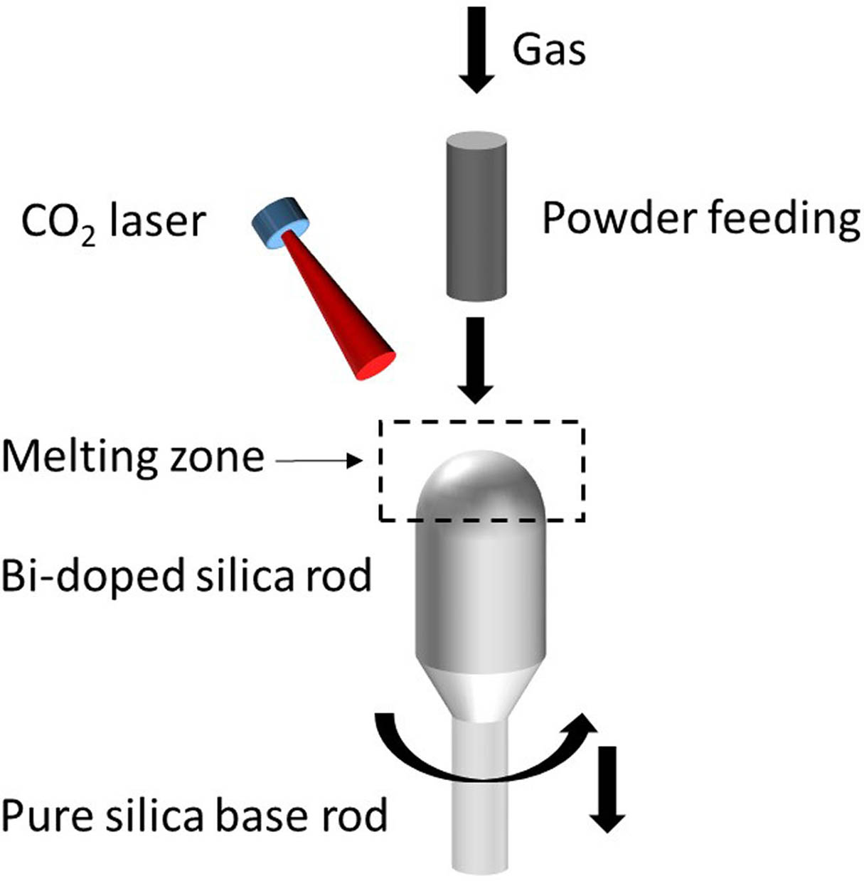
The Bi-doped silica glass fabrication setup in this Letter is shown in Fig. 1. Firstly, according to the composition of 0.5 mol% (99.99%), 2.5 mol% (99.99%), and 97 mol% (99.99%), which corresponds to weight percentages of 3.68 wt% , 4.04 wt% , and 92.28 wt% , the weight of raw materials was calculated, respectively, and then mixed uniformly. Secondly, high temperature (about 1000°C) heating was operated for the mixed powder over 24 h to reduce the groups. Afterwards, the laser sintering process was performed within the setup in Fig. 1. The details are as follows.

Figure 1.Experimental setup for Bi-doped silica glass fabrication.
A pure silica base rod was continuously and uniformly heated by a laser source to over 2000°C and then a melting zone was formed. The laser power density was set to be . was applied to carry the powder through the coaxial powder feeding device and then have it gradually deposited on the melting zone layer by layer. The feeding rate was about 0.6 g/min. Under the radiation of the laser, the core materials of , , and were melted and then solidified when leaving the melting zone. The base rod was constantly rotating and moving downwards simultaneously during the whole process. Finally, a cylindrical rod with length of about 9 cm was obtained. A longer silica rod could be obtained if the deposition process continues. Figure 2 shows a Bi-doped glass sample polished into a reddish-brown cuboid.
Figure 2.Bi-doped silica glass sample.
The glass properties were measured by the instruments as follows. The glass sample doping homogeneity was characterized by the energy dispersive spectrometer (EDS, JSM-6701F). The Fourier transform infrared (FTIR) spectrometer (Nicllet 6700) was used to measure the infrared absorption spectra for concentration analysis. The glass absorption spectrum was obtained by a broadband light source and an optical spectrum analyzer (OSA, MAYA2000 Pro, 200–1100 nm). An 808 nm LD was used to pump the Bi-doped glass sample, and the emission spectra were received by another OSA (NIR Quest 256, 900–2500 nm).
Figure 3 depicts the line scanning EDS result of the Bi element in the glass sample. The line scanning range is 0–250 μm. The intensity of Bi is around six, exhibiting small fluctuations along the 250 μm scanning line. To further explore the distribution homogeneity, the area scanning EDS was also performed as shown in Fig. 4. It is clear that no bright spots were observed in the whole area. This provides further evidence of uniform distribution for Bi ions.
Figure 3.EDS line scanning of Bi.
Figure 4.EDS area scanning of Bi.
It is known that high content would introduce much background loss at 1383 nm, which is located within the working wavelength range of the Bi-doped fiber amplifier. Therefore, the FTIR spectrum of the glass sample was measured and plotted in Fig. 5 to characterize the group’s level. The concentration was calculated using the formula below:
Figure 5.FTIR spectrum of the Bi-doped glass sample.
represents molar weight; represents the extinction coefficient constant ([23]); represents the glass density; is the glass thickness. and are the transmission coefficients of baseline and absorption peaks around , respectively. According to the above formula, the content was mathematically deduced to be 29.36 ppm (parts per million). This value is a little higher than that in mature MCVD technology, which is lower than 10 ppm[24]. We ascribed the high groups to direct contact between raw materials and surrounding air during the feeding and deposition process, resulting in extra groups being introduced. In future work, energy and beam distribution optimizations of the laser source as well as a clean room environment need to be applied to reduce groups. Besides, the heating temperature could be increased by higher to get more effective reduction effects.
A broadband light source covering 300–1100 nm was used to measure the absorption spectrum of the Bi-doped glass sample, which is shown in Fig. 6. Four main absorption bands at 300, 500, 700, and 820 nm are similar to the characteristic absorption peaks in other glasses[25]. The strong absorption band at 300 nm was ascribed to the absorption edge of the -containing glass system[21].
Figure 6.Absorption spectrum of the Bi-doped glass sample.
The fluorescence spectrum of the glass sample was also measured using the setup in Fig. 7. An 808 nm LD was used as the pump source. After collimating and focusing on the target sample, the emission light was collected by an OSA through a collimation lens. A long-pass filter was inserted before the OSA to remove the pump light, which would cause the second diffraction at 1600 nm.
Figure 7.Experimental setup for emission spectrum measurement of the glass sample.
Figure 8 displays the normalized NIR emission spectrum from 900 to 2000 nm under excitation of an 808 nm LD. The emission peak wavelength was at 1249 nm ([14]) for 5 W pump power, corresponding to FWHM of 418 nm. It is much broader than those in silica glasses fabricated by other methods (262 nm in MCVD[14], 263 nm in NPG[22], and about 100 nm in sol-gel[18]). The reason for such a broad bandwidth in our method might be attributed to the difference in the heat treatment history during the fabrication process for different methods[26,27]. The active center itself or its local environment would be modified under the influences of different high temperatures. Detailed mechanisms on this issue still need to be further explored. Nevertheless, the results give the evidence that the Bi-doped silica glass prepared by our method is promising for realizing broadband transmission or use as an ultra-broadband light source. Better broadband emission could be expected if the fabrication process is optimized. The next work would be the exploration and optimization of doping concentration, sintering temperature, reduction of content, etc.
Figure 8.NIR emission spectrum of Bi-doped silica glass under 808 nm LD excitation.
In conclusion, we proposed a new method for fabricating broadband Bi-doped silica glass using laser additive manufacturing. The Bi ions were homogeneously doped into the silica matrix. A broadband emission from 1000 to 1600 nm was obtained, corresponding to 1249 nm emission peak and over 400 nm FWHM value. The results demonstrate that the proposed method is feasible and promising to get homogeneous Bi-doped core material with broadband emission, which shows great potential in next generation broadband amplification for optical communication systems.
References
[1] M. Düser, 1(2011).
[2] Z. Wang, Y. Xie, S. Huang, H. Zhou, R. Liu, Z. Liu, M. Wang, W. Qi, Q. Tian, L. Kong, C. Tu, Y. Li, H. Wang. Chin. Opt. Lett., 17, 1200601(2019).
[3] S. Xu, S. Dai, J. Zhang, L. Hu, Z. Jiang. Chin. Opt. Lett., 2, 106(2004).
[4] Z. Zhang, C. Guo, L. Cui, Y. Zhang, C. Du, X. Li. Chin. Opt. Lett., 17, 100604(2019).
[5] W. Huang, H. Ming, J. Xie, X. Chen, A. Wang, L. Lu. Chin. Opt. Lett., 1, 311(2003).
[6] Y. Fujimoto, M. Nakatsuka. Appl. Phys. Lett., 82, 3325(2003).
[7] S. Zhou, H. Dong, H. Zeng, G. Feng, H. Yang, B. Zhu, J. Qiu. Appl. Phys. Lett., 91, 061919(2007).
[8] S. Zhou, N. Jiang, B. Zhu, H. Yang, S. Ye, G. Lakshminarayana, J. Hao, J. Qiu. Adv. Funct. Mater., 18, 1407(2008).
[9] V. V. Dvoyrin, V. M. Mashinsky, E. M. Dianov, A. A. Umnikov, M. V. Yashkov, A. N. Guryanov, 949(2005).
[10] E. M. Dianov, A. V. Shubin, M. A. Melkumov, O. I. Medvedkov, I. A. Bufetov. J. Opt. Soc. Am. B, 24, 1749(2007).
[11] I. A. Bufetov, S. V. Firstov, V. F. Khopin, O. I. Medvedkov, A. N. Guryanov, E. M. Dianov. Opt. Lett., 33, 2227(2008).
[12] S. V. Firstov, S. V. Alyshev, K. E. Riumkin, M. A. Melkumov, E. M. Dianov, ASu3C.3(2015).
[13] N. K. Thipparapu, A. A. Umnikov, P. Barua, J. K. Sahu. Opt. Lett., 41, 1518(2016).
[14] J. Li, L. Liao, Y. Chu, P. Liu, H. Li, J. Peng, N. Dai. J. Non-Crystall. Solids, 431, 159(2016).
[15] P. Liu, L. Liao, Y. Chu, Y. Wang, X. Hu, J. Peng, J. Li, N. Dai. Acta Phys. Sin., 64, 224220(2015).
[16] Y. Chu, Y. Yang, L. Liao, Y. Liu, Y. Ma, X. Hu, Y. Wang, Y. Xing, J. Peng, H. Li, N. Dai, J. Li, L. Yang. ACS Photon., 5, 4014(2018).
[17] L. D. Iskhakova, V. M. Mashinsky, F. O. Milovich, V. V. Velmiskin, E. A. Plastinin, S. V. Firstov, M. V. Lukashova, P. A. Somov, E. M. Dianov. J. Non-Crystall. Solids, 503–504, 28(2019).
[18] I. Razdobreev, H. E. Hamzaoui, L. Bigot, V. Arion, G. Bouwmans, A. L. Rouge, M. Bouazaoui. Opt. Express, 18, 19479(2010).
[19] Z. Fang, S. Zheng, W. Peng, H. Zhang, Z. Ma, G. Dong, S. Zhou, D. Chen, J. Qiu. J. Am. Ceramic Soc., 99, 856(2016).
[20] Y. Chu, Q. Hu, Y. Zhang, Z. Gao, Z. Fang, L. Liu, Q. Yan, Y. Liu, S. Sun, G.-D. Peng, E. Lewis, J. Ren, J. Zhang. Adv. Opt. Mater., 6, 1800024(2018).
[21] Y. Fujimoto, M. Nakatsuka. Jpn. J. Appl. Phys., 40, L279(2001).
[22] R. Zhao. The Research on Wide-band Luminescent Glass and Fiber Based on Nanoporous Silica Glass(2019).
[23] J. Kirchhof, S. Unger, A. Schwuchow, S. Jetschke, V. Reichel, M. Leich, A. Scheffel. Proc. SPIE, 7598, 75980B(2010).
[24] Y. Wang, N. K. Thipparapu, S. Wang, P. Barua, D. J. Richardson, J. K. Sahu. Opt. Lett., 44, 5650(2019).
[25] M. Peng, N. Zhang, L. Wondraczek, J. Qiu, Z. Yang, Q. Zhang. Opt. Express, 19, 20799(2011).
[26] T. Haruna, M. Kakui, T. Taru, S. Ishikawa, M. Onishi, MC3(2005).
[27] V. G. Truong, L. Bigot, A. Lerouge, M. Douay, I. Razdobreev. Appl. Phys. Lett., 92, 041908(2008).