Abstract
We have developed a cost-effective and highly compact 100-Gb/s coarse wavelength division multiplexing (CWDM) transmitter optical subassembly (TOSA) using lens-free hybrid integration. To achieve large alignment tolerances, distributed feedback laser diodes (DFB-LDs) are butt-coupled to a four-channel silica-based planar lightwave circuit (PLC) arrayed waveguide grating, with the silicon sub-mounts and PLC adhesively bonded. Then, a flexible printed circuit is employed to connect the internal DFB-LDs and the exterior of the TOSA package for radiofrequency signal transmission, eliminating the expensive ceramic feed-through. The packaged CWDM TOSA, which is in size, shows a side-mode suppression ratio of , a 3 dB bandwidth of , and error-free transmission with an average optical output power of and dynamic extinction ratio of at 25.78125 Gb/s over a 10 km single-mode fiber for all four lanes.1. INTRODUCTION
With the rapid growth of data traffic in local area networks and wireless mobile communications, high-speed, low-cost, and highly compact transmitter optical subassemblies (TOSAs) are essential and have attracted substantial interest in recent years. To increase the transmission capacity, multi-lane configurations are utilized, such as wavelength division multiplexing and parallel single-mode four-lane. 100 Gbit Ethernet (100-GbE), standardized as IEEE 802.3ba in 2010 [1], employs four electro-absorption modulator integrated lasers (EMLs) with a wavelength channel spacing of 800 GHz in the O-band for the 10 or 40 km transmission over a single-mode fiber (SMF). So far, various 100-GbE TOSAs have been developed to meet the standards using silica planar lightwave circuit (PLC) hybrid integration [2–5] and InGaAsP-based monolithic integration [6,7]. In contrast to InGaAsP-based multiplexers, arrayed waveguide gratings (AWGs) based on silica-PLC have the advantages of low loss, relaxed fabrication tolerance, and thermal insensitivity. For data center applications, cost effective and highly compact TOSAs with a relatively short transmission distance are required. In this case, 100 GbE transceivers have recently been defined in the multi-source agreement (MSA) [8] for 2 and 10 km transmission using distributed feedback laser diodes (DFB-LDs) and coarse wavelength division multiplexing (CWDM). The DFB-LDs are directly modulated at 25.78125 Gb/s for the four lanes with a 20 nm wavelength channel spacing. Due to the broad bandwidth of each lane, the CWDM technique relaxes the requirement of wavelength accuracy of DFB-LDs, and thermoelectric coolers (TECs) are no longer needed to stabilize the wavelength as the temperature fluctuates. Thus, the integration is simplified and the cost can be greatly reduced compared to the TOSAs in Refs. [2–7,9].
100 Gb/s silicon photonics CWDM4 optical transceivers have been developed using hybrid silicon lasers, silicon modulators, and an echelle-grating-based multiplexer on a silicon platform [10,11]. However, the cost of the silicon-based TOSA is not really low, because of the complicated integration of four hybrid lasers, stringent fabrication requirements, and thermal sensitivity of silicon waveguides [12,13]. At present, 100-GbE TOSAs using thin-film filters [9] and silica-PLC hybrid integration are still competitive and prevalently chosen for their low cost. Compared to the thin-film filters, silica-PLC hybrid integration is more promising for the optical interconnect in data centers due to its simple assembly and compact size. Recently, a 100 Gb/s CWDM4 TOSA has been demonstrated by a hybrid assembly of silicon-based modulators and electronics, a silica-PLC multiplexer, and an MEMS carrier with individual InP lasers [14]. As reported in Ref. [15], a hybrid integrated O-band CWDM4 silica-PLC TOSA is realized with a 3 dB bandwidth broader than 18.15 GHz for all the lanes, but the data rates are not mentioned. In these TOSAs, the coupling between the lasers and PLC is through a lens for each lane, which requires a very tight lens positional tolerance (approaching the submicrometer order) and thus limits the process yield. Although submicrometer lens alignment can be realized by using high-power laser irradiation [4,9] and micromechanical techniques [14,16], the cost is relatively high for mass fabrication. Moreover, for the lens-coupling schemes, the large lens size might cause limitations when further miniaturization of the optical module is needed. Another scheme is coupling through a butt joint, in which it is unnecessary to use any lens; this has been employed in many 100-GbE TOSAs with a TEC [2,3,5]. However, the UV-curable adhesive could spread to the laser facet after butt-coupling integration, which may cause unpredictable degradation of laser performance in mass production.
To further reduce the cost, the packaging of TOSAs can also be improved. Recently, a low-cost EML TOSA operating at 25 Gb/s was demonstrated using all-in-one flexible printed circuit (FPC) wiring [17], eliminating the expensive ceramic sub-mount and feed-through. However, for this TOSA, the EML burn-in could be problematic, as there is no sub-mount and the bare EML is too small.
Sign up for Photonics Research TOC. Get the latest issue of Photonics Research delivered right to you!Sign up now
In this paper, we have demonstrated a cost-effective hybrid-integrated 100 Gb/s CWDM4 TOSA using four uncooled DFB-LDs and a silica-PLC-based AWG multiplexer. The DFB-LD and silica-PLC are coupled through a butt joint, and the adhesive is applied between the silicon sub-mount and silica-PLC. Moreover, to reduce the packaging cost, an FPC is used to replace the expensive ceramic feed-through in our TOSA for high-speed signal transmission. The packaged TOSA is only in size. For each lane, the side-mode suppression ratio (SMSR) is larger than 40 dB, and the 3 dB bandwidth is broader than 18 GHz. The TOSA exhibits error-free transmission over a 10 km SMF, with an average output power () exceeding 0 dBm and a dynamic extinction ratio (DER) of over 4.0 dB at 25.78125 Gb/s when all four lanes are simultaneously operated, satisfying the specifications of 100-G CWDM4 MSA.
2. TOSA CONFIGURATION
Figure 1 shows the structure of the proposed CWDM TOSA. It contains a silica-PLC AWG integrated with a pigtail SMF, four discrete DFB-LD subassemblies, a metal bench, a heat sink, and an FPC. Four DFB-LD subassemblies are butt-coupled to the PLC, which is attached to the top of a metal bench made of ferronickel. The input facet of the PLC is slant-polished to reduce the optical back-reflection. Then, the metal bench is tilted in the horizontal direction for coaxial alignment between the PLC and DFB-LDs. As seen, an FPC is extended from the inside DFB-LDs to the exterior of the TOSA. This avoids the need for high-cost ceramic feed-through and reduces the number of signal-transmission nodes, resulting in low manufacturing cost and high-frequency performance for the TOSA. Finally, to prevent moisture penetration, the slits on the front and rear sidewalls of the metal box are sealed with elastic epoxy.
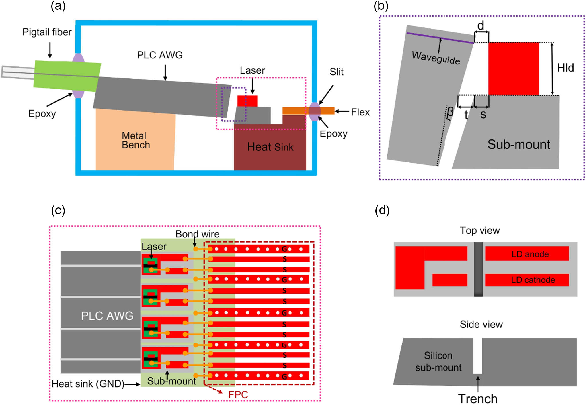
Figure 1.Proposed TOSA configuration. (a) Cross-sectional view of the TOSA. (b) Side view of the butt-coupling region. (c) Top view of the coupling region with the DFB-LDs connected with an FPC. (d) Top and side views of silicon sub-mount.
As shown in Fig. 1(b), the input facet of the PLC is polished at an angle , and the distance between the DFB-LD and PLC waveguide is . Coupling efficiency (CE), back-reflection, and alignment tolerance are usually used to evaluate the butt-coupling scheme. An optical ray-tracing method is adopted to calculate the CE and back-reflection. In the simulation, we assume that the far-field pattern from the DFB-LD has a full width at half maximum (FWHM) of 35° and 25° for the vertical and horizontal directions, respectively. Meanwhile, the far-field pattern from the PLC waveguide has an FWHM of 12° for both vertical and horizontal directions. The input facet of the PLC is coated with 0.2% anti-reflection (AR) coating. It is found that when is 5 μm and is 8°, the back-reflection is less than and the CE is around , which can meet the requirements of TOSA integration. Then, the tilted angle of the metal bench is determined as 3.5° to the horizontal direction. We use and to represent the distance from the DFB-LD to the sub-mount edge, and the gap between the sub-mount and PLC, respectively.
When applying UV-curable adhesive to bond the sub-mounts and PLC, is preferred to be 10–20 μm. Then, is determined as 7.38–17.38 μm. A high-precision die bonder can be incorporated to position the DFB-LD with a height of 110 μm. To achieve a high yield, large alignment tolerance in the assembling direction is of great importance. Here, the DFB-LD and PLC are assembled in the horizontal direction. Figure 2 shows the calculated coupling efficiency as a function of . It is seen that the CE decreases from to as increases from 5 to 8.5 μm, indicating 1 dB alignment tolerance of 3.5 μm, which is much larger than that of the lens-based solutions (submicrometer) [4].

Figure 2.Coupling efficiency as a function of for the proposed butt-coupling configuration.
As seen in Fig. 1(c), the radiofrequency (RF) transmission line of the FPC has a ground–signal–signal–ground structure with periodic via-holes on the ground wires. The FPC was fabricated using polyimide (dielectric constant ) type flexible copper-clad laminate. The FPC structure was designed using an ANSYS High Frequency Structure Simulator and Agilent Advanced Design System. The FPC is 9.5 mm long. The width and pitch of the signal wires are 0.28 and 0.50 mm, respectively. The RF return loss (S11) and insertion loss (S21) of the FPC were found to be more than 25 dB and less than 0.4 dB, respectively, at 20 GHz.
The DFB-LDs are fixed on the silicon sub-mounts designed for 25 Gb/s transmission. As shown in Fig. 1(d), the sub-mount has two parts separated by a trench. The bonding pads of the two parts are electrically connected by wire bonding. Then, the direct current probe is placed on the bond pads of the right part for DFB-LD power supply. The sub-mount design can shorten the TOSA length, as the right part will be removed at last. The heat sink is made of copper–tungsten (CuW) with a thermal conductivity of , and thus can efficiently dissipate the heat. For optimal high-frequency performance, the heat sink is designed with a step to keep the wire bonding pads of FPC and silicon sub-mount on the same level.
As shown in Fig. 3(a), the silica-PLC AWG chip has a size of and an input port pitch of 1.6 mm. The refractive indices of the cladding () and core (–) are 1.4475 and 1.4692, respectively, and the core size of the PLC waveguide is [see Fig. 3(b)]. The PLC can multiplex four CWDM lanes with central wavelengths located at 1271, 1291, 1311, and 1331 nm. The measured FWHM of the PLC input port is about 10° for both vertical and horizontal directions. Figure 3(c) plots the transmission spectra of the AWG. It is observed that the peak insertion loss is lower than 2.5 dB and the 1 dB bandwidth is wider than 10 nm, satisfying the TOSA assembly requirement. Moreover, the output waveguide is coupled to a pigtail SMF that introduces around 0.5 dB coupling loss.
Figure 3.(a) Schematic of the silica-PLC AWG. (b) Scanning electron microscope image of the PLC waveguide before the depositing of cladding. (c) Transmission spectra of the silica-PLC AWG.
3. BUTT-COUPLING ALIGNMENT TOLERANCE
Compared with the lens coupling, the proposed butt coupling has a larger assembling tolerance. For illustration, we have performed alignment tolerance measurements for our butt-coupling and lens-coupling schemes, as plotted in Figs. 4(a) and 4(b), respectively. In Fig. 4(a), the DFB-LD subassemblies and PLC are adhesively bonded at the end facets, and the aligned position error is mainly in the horizontal direction due to the variation of adhesive thickness after UV curing. In contrast, the main position error is in the vertical direction for the lens coupling, since the lens is adhesively bonded to the top of the metal shim, as shown in Fig. 4(b). Here, we utilized an aspheric lens with a magnification of 4, which can convert the high numerical aperture (NA, ) of the DFB-LD waveguide to the low NA (). The measurement was conducted on a six-axis Thorlabs automatic alignment station. The direct current probe was placed on the sub-mount for the DFB-LD power supply, and the pigtail SMF was connected to a power meter. Figure 4(c) shows the relative CE as a function of the position variation in the horizontal and vertical directions for the butt-coupling and lens-coupling schemes, respectively. For the tolerance measurement of the butt coupling, was tuned from 5 to 10 μm with a step of 0.5 μm. For the lens-coupling scheme, the distance between the DFB-LD and the lens was 0.25 mm, and the distance between the lens and the PLC was 3.5 mm. During the tolerance measurement of the lens coupling, the vertical position of the lens was varied from 0 to 4 μm with a step of 0.5 μm. It is found that the 1 dB tolerance is more than 3 μm for the proposed butt coupling, while it is about 0.4 μm for the lens coupling. The vertical variation of lens position causes a magnified misalignment between the lens and the DFB-LD/PLC. In addition, we measured the output power degradation for four lanes in PLCs after the UV curing, as shown in Fig. 4(d). It is seen that the power degradation of each lane is lower than 0.5 dB for our scheme, while it is larger than 3 dB for the lens coupling. The results indicate that the manufacturing yield of our TOSA can be higher, and the cost is lower, due to the relatively large assembling tolerances.
Figure 4.Measurement setups for (a) the proposed scheme and (b) the lens-based solution. (c) Relative CE as a function of position variation. (d) Output power degradation after UV adhesive curing.
4. TOSA FABRICATION
The TOSA fabrication processes include the assembling of the PLC sub-block, attachment of the CuW heat sink and FPC, and elastic epoxy sealing of the slits. The DFB-LD was first eutectic-bonded to the silicon sub-mount. Then, wire bonding was processed to connect the pads of the DFB-LD and silicon sub-mount. The PLC was manually fixed on the metal bench with epoxy. Consequently, the DFB-LD subassemblies were actively aligned and adhesively bonded to the PLC one by one. A six-axis Thorlabs automatic alignment station was used for the active alignment. During the aligning, it is crucial to find the origin position (i.e., ), which is defined as the location where the output power from the PLC reaches the maximum. Once this was found, the DFB-LD subassembly was moved away 5 μm in the longitudinal direction, and then aligned in the transverse directions. The aligned PLC sub-block is shown in Fig. 5(a). The front facet of the DFB-LD is AR coated to reduce the reflection at the DFB-LD/air interface. Figure 5(c) shows that the gap between the silicon sub-mount and silica-PLC is filled with UV-curable adhesive, which does not spread to the DFB-LD front facet. The clean DFB-LD facet guarantees low reflection at the interface, since the refractive index of the adhesive is about 1.5, quite different from that of air.
Figure 5.(a) Photograph of the fabricated silica-PLC sub-block. (b) External dimension of the developed TOSA. (c) Top and side views of the butt-coupling region.
The CuW heat sink and FPC were assembled using silver epoxy. The heat sink was first attached to the bottom of the metal box, and then an FPC was attached to the step of the heat sink. The silica-PLC sub-block was then attached to the metal box and heat sink. A thermal conductive epoxy was applied between the sub-mount and heat sink. Thus, the heat from the DFB-LD can be dissipated quickly to the metal box through the heat sink. Finally, to protect the TOSA from moisture penetration, a piece of metal cover was sealed to the metal box by elastic epoxy, and the slits were also sealed. The fabricated TOSA has a size of , which is compact enough for the CFP4 and QSFP28 form-factors [18,19].
5. EXPERIMENTAL RESULTS
Next, the packaged TOSA was characterized at a temperature of 25°C. Figure 6(a) shows the output power as a function of the injection current by probing on the FPC. As seen, the threshold current is about 5 mA, and there are no kinks in the curve for each lane of the packaged TOSA. Moreover, for each lane, the output power increases steadily and monotonously as the current increases, and exceeds 1 mW (0 dBm) with the injection current of 30 mA. At the injection current of , the slope efficiency starts to fall slightly, which is possibly attributed to the non-perfect thermal contact between the silicon substrate and CuW heat sink. Nevertheless, the impact is limited, and the TOSA still performs quite well, as shown in the following paragraphs. The obtained coupling efficiencies between the DFB-LD and PLC are , , , and for Lanes 0, 1, 2, and 3, respectively, which are close to the simulated value. Figure 6(b) shows the lasing spectra of the integrated TOSA at a current of 40 mA. As seen, single-mode lasing is obtained, and the lasing wavelengths are 1272.7, 1292, 1311.2, and 1330.8 nm. The SMSRs are 41.1, 43.5, 42.0, and 43.2 dB for Lanes 0, 1, 2, and 3, respectively. These results indicate that the back-reflection is low enough, and our coupling scheme does not degrade the laser stability.
Figure 6.(a) Output power of the packaged TOSA as a function of injection current for the four lanes. (b) Lasing spectra of the TOSA at an injection current of 40 mA.
The small signal electro-optic responses of the TOSA were measured using a 65 GHz vector network analyzer (VNA), 50 GHz photodetector, and an RF probe. The RF signal from the VNA was injected by directly probing the FPC through an RF probe. All the DFB-LDs operated at the injection current of 35 mA. As shown in Fig. 7, the 3 dB bandwidths of S21 are 18.0, 19.7, 20.5, and 22.5 GHz for Lanes 0, 1, 2, and 3, respectively. The difference of 3 dB bandwidth results primarily from the discrepancy of the employed DFB-LDs.
Figure 7.Small-signal frequency response of S21 when each DFB-LD was discretely driven.
Back-to-back (BtoB) transmission experiments were performed using signal patterns of a 25.78125 Gb/s non-return-to-zero, pseudo-random bit sequence. The data were obtained by driving the DFB-LDs with a peak-to-peak current of for all the lanes simultaneously, when the bias currents all were 32 mA. Figure 8 shows the eye diagram for each lane through a fourth-order Bessel filter. It is seen that sufficiently clear eye openings are obtained with a larger than 1.0 mW and DER more than 4.0 dB for all the lanes. Moreover, the eye mask margins are 41.7%, 32.5%, 38.4%, and 40.1%, and the optical modulation amplitudes (OMAs) are 0.41, , 0, and 0.79 dBm for Lanes 0, 1, 2, and 3, respectively.
Figure 8.Eye diagrams for the BtoB transmission of the TOSA.
Figure 9 shows the bit-error-ratio (BER) curves for BtoB and after a 10 km transmission over an SMF when all the lanes were driven simultaneously using the eye diagram condition shown in Fig. 8. The optical signal from each lane was extracted with a tunable wavelength filter, and then received by a photoreceiver integrated with a p-i-n photodiode and BER tester. As seen, for the BtoB transmission, the receiver sensitivities at a BER of are , , , and for Lanes 0, 1, 2, and 3, respectively. Moreover, after the 10 km transmission, the power penalties are less than 0.5 dB, and error-free transmission is achieved for all the lanes.
Figure 9.Bit error ratio characteristics for BtoB and after a 10 km transmission, when all four lanes were driven using the eye diagram condition shown in Fig. 8.
Overall, the fabricated CWDM TOSA exhibits SMSRs of over 41 dB, values of over 0 dBm, OMAs of over , DERs of over 4.0 dB, and four- error-free transmission over a 10 km SMF. Thus, it can meet the CWDM4 MSA specifications (e.g., , , , and ). Due to the low cost and compactness, our CWDM TOSA is a promising candidate for 100 GbE transceivers.
6. CONCLUSION
In summary, we have developed a cost-effective and highly compact hybrid-integrated 100 Gb/s CWDM TOSA. The directly modulated DFB-LDs and silica-PLC AWG are butt-coupled with large alignment tolerances. To reduce the packaging cost and enhance high-frequency performance, an FPC was used to directly connect the DFB-LDs and exterior of the TOSA. The proposed TOSA has successfully realized a error-free transmission over a 10 km SMF with and under all-lane simultaneous operation at 25°C. This hybrid integration technique is an effective way to fabricate a compact and cost-effective multi-lane CWDM TOSA for a 100 GbE transceiver or a future 400 GbE transceiver.
References
[1] . IEEE P802.3ba 40Gb/s and 100Gb/s Ethernet Task Force.
[2] T. Ohyama, Y. Doi, W. Kobayashi, S. Kanazawa, K. Takahata, A. Kanta, T. Kurosaki, T. Tanaka, T. Ohno, H. Sanjoh, T. Hashimoto. Compact hybrid integrated 100-Gb/s transmitter optical sub-assembly using optical butt-coupling between EADFB lasers and silica-based AWG multiplexer. J. Lightwave Technol., 34, 1038-1046(2016).
[3] T. Ohyama, Y. Doi, W. Kobayashi, S. Kanazawa, T. Tanaka, K. Takahata, A. Kanta, T. Kurosaki, T. Ohno, H. Sanjoh, T. Hashimoto. Compact hybrid-integrated 100-Gb/s TOSA using EADFB laser array and AWG multiplexer. IEEE Photon. Technol. Lett., 28, 802-805(2016).
[4] T. Murao, N. Yasui, K. Mochizuki, M. Shimono, H. Kodera, D. Morita, T. Yamatoya, H. Aruga. Lens alignment technique using high-power laser for hybrid integrated multi-channel transmitter optical subassembly. IEEE Photon. Technol. Lett., 25, 1958-1960(2013).
[5] Y. Baek, Y. T. Han, C. W. Lee, D. H. Lee, O. K. Kwon, J. W. Shin, S. H. Park, Y. A. Leem. Optical components for 100-G Ethernet transceivers. Opto-Electronics and Communications Conference (OECC), 4D1-2(2012).
[6] S. Kanazawa, T. Fujisawa, N. Nunoya, A. Ohki, K. Takahata, H. Sanjoh, R. Iga, H. Ishii. Ultra-compact 100-GbE transmitter optical sub-assembly for 40-km SMF transmission. J. Lightwave Technol., 31, 602-608(2013).
[7] T. Fujisawa, S. Kanazawa, Y. Ueda, W. Kobayashi, K. Takahata, A. Ohki, T. Ito, M. Kohtoku, H. Ishii. Low-loss cascaded Mach-Zehnder multiplexer integrated 25-Gbit/s × 4-lane EADFB laser array for future CFP4 100-GbE transmitter. IEEE J. Quantum Electron., 49, 1001-1007(2013).
[8] http://www.cwdm4-msa.org. http://www.cwdm4-msa.org
[9] T. Murao, N. Yasui, T. Shinada, Y. Imai, K. Nakamura, M. Shimono, H. Kodera, Y. Morita, A. Uchiyama, H. Koyanagi, H. Aruga. Integrated spatial optical system for compact 28-Gb/s×4-lane transmitter optical subassemblies. IEEE Photon. Technol. Lett., 26, 2275-2278(2014).
[10] B. Koch, A. Alduino, L. Liao, R. Jones, M. Morse, B. Kim, W. Lo, J. Basak, H. Liu, H. Rong, M. Sysak, C. Krause, R. Saba, D. Lazar, L. Horwitz, R. Bar, S. Litski, A. Liu, K. Sullivan, O. Dosunmu, N. Na, T. Yin, F. Haubensack, I. Hsieh, J. Heck, R. Beatty, J. Bovington, M. Paniccia. A 4 × 12.5 Gbps CWDM Si photonics link using integrated hybrid silicon lasers. CLEO: Science and Innovations, CThP5(2011).
[11] . Intel Silicon Photonics Products.
[12] A. V. Krishnamoorthy, X. Zheng, D. Feng, J. Lexau, J. F. Buckwalter, H. D. Thacker, F. Liu, Y. Luo, E. Chang, P. Amberg, I. Shubin, S. S. Djordjevic, J. H. Lee, S. Lin, H. Liang, A. Abed, R. Shafiiha, K. Raj, R. Ho, M. Asghari, J. E. Cunningham. A low-power, high-speed, 9-channel germanium-silicon electro-absorption modulator array integrated with digital CMOS driver and wavelength multiplexer. Opt. Express, 22, 12289-12295(2014).
[13] S. Tao, Q. Huang, L. Zhu, J. Liu, Y. Zhang, Y. Huang, Y. Wang, J. Xia. Athermal 4-channel (de-)multiplexer in silicon nitride fabricated at low temperature. Photon. Res., 6, 686-691(2018).
[14] L. Soldano, J. Kubicky, D. Ton, J. Wendland, M. Allen, A. Grant, B. Pezeshki. Multi-wavelength 100-Gb/s silicon photonics based transceiver with silica mux/demux. Optical Fiber Communication Conference, Th3B.1(2017).
[15] J. An, J. Zhang, L. Wang, K. Zhu, B. Sun, Y. Li, J. Hou, J. Li, Y. Wu, Y. Wang, X. Yin. Hybrid silica coarse wavelength-division multiplexer transmitter optical subassembly. Opt. Eng., 57, 017108(2018).
[16] B. Pezeshki, J. Heanue, D. Ton, T. Schrans, S. Rangarajan, S. Zou, G. W. Yoffe, A. Liu, M. Sherback, J. Kubicky, P. Ludwig. High performance MEMS-based micro-optic assembly for multi-lane transceivers. J. Lightwave Technol., 32, 2796-2799(2014).
[17] Y. T. Han, O. K. Kwon, D. H. Lee, C. W. Lee, Y. A. Leem, J. U. Shin, S. H. Park, Y. Baek. A cost-effective 25-Gb/s EML TOSA using all-in-one FPCB wiring and metal optical bench. Opt. Express, 21, 26962-26971(2013).
[18] http://www.cfp-msa.org. http://www.cfp-msa.org
[19] SFF Committee. QSFP+ 28 Gb/s 4X pluggable transceiver solution (QSFP28)(2015).


