Abstract
The optical saturation characteristics in the germanium-on-silicon (Ge-on-Si) photodetector are studied for the first time, to the best of our knowledge. The relationship between the optical saturation characteristics and the optical field distribution in the Ge layer is illustrated by the simulation. This theory is verified by comparative experiments with single-injection and dual-injection structures. The dual-injection photodetector with a more balanced and uniform optical field distribution has a 13% higher responsivity at low optical power and 74.4% higher saturation current at 1550 nm. At higher optical power, the bandwidth of the dual-injection photodetector is five times larger than that of the single-injection photodetector.In recent years, silicon (Si)-based photoelectrons have gathered extensive interest, owing to their low cost and easy integration[1–4]. To date, a large amount of work on Si-based germanium (Ge) photodetectors and a series of photodetectors with excellent properties have been reported[5–19]. However, up to now, the saturation characteristics of the Ge-on-Si photodetector and related mechanisms have not been investigated. In this Letter, we study the saturation characteristics of a single-injection photodetector and a dual-injection photodetector[20], which have different light-field distributions. The saturation process was shown by experiments, and the mechanism was explained by the simulation. The experiments show the function of the responsivity with the change of the optical power and the light saturation characteristics of these two photodetectors. The bandwidth change of the two photodetectors with the increase of the signal optical power has also been shown in the experiments. The distribution of the light field in the two structures was studied by simulation. The simulation also accounts for the reason that the saturation region of the absorption layer is changed with the increase of the incident optical power.
First, the wafer was lightly doped to obtain a -type region and then heavily doped to obtain good ohmic contacts. Prior to Ge epitaxy, rapid thermal annealing (RTA) at 1030°C for 5 s was performed to activate the dopants. Then, the Ge layer was selectively grown using the two-step-growth approach. The thickness of the Ge layer was designed as 500 nm. Subsequently, N++ implantation was undertaken to form an -type region and obtain good ohmic contacts, and the dopants in Ge were activated by another RTA process at 500°C for 5 min. Then, an approximately 1 μm upper cladding oxide was deposited for surface passivation. Finally, aluminum ground–signal–ground electrodes were formed. The thickness of the Si waveguide was 220 nm. The rib waveguide was 1.8 μm wide with a 60 nm slab thickness, which can well confine the mode in the waveguide.
The responsivity was measured by the direct-current (DC, Keithley 2611 A System SourceMeter) electrical source. The sensitivity could reach 1 nA. The DC electrical source applied the DC bias on the photodetector and tested the DC current at the same time. The 3 dB bandwidth was measured using a vector network analyzer (VNA, Keysight PNA-X Network Analyzer N5247 A), which provided measurement capability to 67 GHz. A high speed radio frequency (RF) signal generated from the VNA was applied to a high performance modulator (with 40 GHz bandwidth). The modulated light at 1550 nm was coupled to the device using a lensed fiber, and the electrical output was measured with 50 Ω high speed RF probes.
Sign up for Chinese Optics Letters TOC. Get the latest issue of Chinese Optics Letters delivered right to you!Sign up now
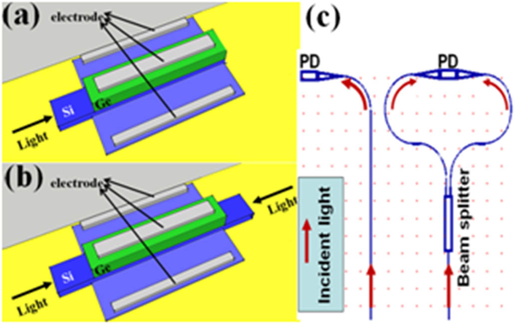
The structures of the dual-injection, single-injection, and Si waveguides are shown in Fig. 1. These two photodetectors differ in that the single-injection photodetector injects light from one end, whereas the dual-injection photodetector injects light from both ends. The light beam of the dual-injection photodetector is separated by a 3 dB beam splitter and then injected into the photodetector at the two ends of the Si waveguide. The size of the 3 dB beam splitter is , and the loss is only 2.3% when tested at 1550 nm.

Figure 1.Three-dimensional schematic of the Ge-on-Si positive-intrinsic-negative (PIN) waveguide photodetectors with the (a) single-injection structure, (b) dual-injection structure, and (c) waveguide structure in the layout.
Figure 2 shows the simulation of the light-field distribution of the single- and dual-injection photodetectors obtained using the finite-difference time-domain (FDTD) method. In the single-injection photodetector, the light near the injection side is very large, and it is very small far from the injection side. In addition, the light field is only distributed in a portion of the Ge absorption layer, which could reduce the effective absorption length, as shown in Fig. 2(a). In contrast, the light-field distribution of the dual-injection photodetectors is more balanced, as shown in Fig. 2(b), and is more uniform and wide because not only is the optical power divided at both ends of the injection, but also the different ends of the light can form a stable and dense superposition and interference field, which can increase the effective absorption area. Because of the symmetric incidence and the mutual interference of light in the dual-injection structure, as shown in Fig. 2(b), the configuration has a more uniform and wide light-field distribution, which can increase the length of the effective absorption zone. We calculated the response-area ratio of the single- and dual-injection photodetectors as 31.65% and 58.72%, respectively, from the simulation result.
Figure 2.Top view of the light-field distribution in the Ge absorption layer of the (a) single- and (b) dual-injection photodetectors by the FDTD method; the red box represents the Ge-absorption area.
We tested the photocurrent of the single- and dual-injection Ge-on-Si waveguide photodetectors using different light power. The results are shown in Fig. 3. When the input optical power of the single-injection structure was lower than 4.43 mW, and that of the dual-injection structure was lower than 9.97 mW, the photocurrent increased almost linearly with the increase in the optical power. In this linear range, the dual-injection photodetector had higher responsivity of 0.88 A/W than the single-injection photodetector, which was 0.78 A/W. After the first-stage linear region, the input optical power of the single-injection structure was larger than 4.43 mW, and that of the dual-injection structure was larger than 9.97 mW, so the photocurrent increased also almost linearly as the injected optical power increased, but the rate slowed down. The increase rates of the dual- and single-injection structures were 0.06 and 0.18 A/W, respectively.
Figure 3.Measured photocurrent as a function of the input light power at 1550 nm for both single- and dual-injection photodetectors.
When the injected optical power of the single-injection structure reached 20.60 mW, and that of the dual-injection structure reached 151.71 mW, the photocurrent reached saturation, and the saturated photocurrents were 5.71 and 9.96 mA, respectively. Both the dual- and single-injection photodetector photocurrents in the two stages increased as the optical power increased. In the unsaturated region, the responsivity of the single- and dual-injection structure is constant as the incident optical power increases. When the incident optical power exceeds the saturation power, the responsivity of the photodetector begins to decrease. This shows that in the Ge photodetector, the responsivity is a value that is a function of the incident optical power and is not a constant value.
In the Ge-on-Si photodetectors, the saturation is mainly due to the carrier-screening effect[21]. When the light intensity is too large, photocarriers cannot be transported in time to cause a stacking effect, thereby generating a saturated photocurrent. In this waveguide photodetector, since the intensity of the light-field distribution is uneven, the entire absorption region does not reach saturation at the same time. Figure 4 shows that the photo-generated carrier saturation area gradually increases as the incident light intensity increases by the simulation. The black area represents the absorption area, and the white area represents the light field, where it could generate the saturation photocurrent. In the first stage (unsaturation), all regions in the Ge absorption layer did not attain saturation. In the second stage (subsaturation), the maximum light intensity of the light field in the Ge absorption layer began to generate the saturation photocurrent. In the third stage (saturation), all regions of the light-field distribution in the photodetector generated the saturation photocurrent. In the saturated region, the photocurrent did not increase as the optical power increased, whereas in the unsaturated region, the light absorption continued to increase as the optical power increased. Therefore, the increase in the photocurrent with the increase in the incident optical power in the second stage was slower than that in the first stage. With the increase in the incident optical power, the saturation region gradually increased, and the unsaturated region gradually decreased until the entire Ge absorption region was saturated. At this point, the photocurrent of the photodetectors was saturated, as shown in Fig. 4. The experimental results show that the dual-injection photodetector had higher responsivity than the single-injection photodetector at low injected optical power and had a higher saturation photocurrent. That is because it has a more uniform and extensive light-field distribution, which is equal to increasing the effective absorption region.
Figure 4.Threshold-enhanced image of the saturated light power in the Ge-absorption layer under different incident light power; the white zone represents the saturation area. The saturation threshold is . (a) Single-injection photodetector. (b) Dual-injection photodetector.
In addition, the single-injection structure showed more drastic alternate between strong and weak light-field distribution in the Ge absorption layer than in the dual-injection structure, which made the trap sites in the Ge/Si heterostructure occupied for longer fractions of time because of the high generation rate of free carriers. This process decreased the recombination rate of minority carriers, reducing the responsivity[22].
Figure 5 shows the bandwidth characteristics of the single- and dual-injection photodetectors under different luminous optical power. Similar to the responsivity characteristic, the bandwidths of the single- and dual-injection structures decreased as the injected optical power increased. However, the decrease rate in the bandwidth of the dual-injection photodetector was much smaller than that of the single-injection photodetector with the increase in the incident optical power. The experiments show that when the injection light power was less than 5 mW in the single-injection photodetector and 10 mW in the dual-injection photodetector, the bandwidth was almost constant with the change in the injection light power. Before the first-stage saturated light power was obtained, the dual-injection bandwidth was , and the single-injection bandwidth was . The second-stage saturated light power of the single-injection photodetectors ranged from 5 to 25 mW, and the bandwidth decreased to 3.7 GHz. As the incident light power further increased, the bandwidth remained almost constant. For the dual-injection structure, when the incident optical power was larger than 10 mW, the bandwidth decreased as the optical power increased. When the incident optical power reached 50 mW, the bandwidth decreased to 15.5 GHz.
Figure 5.Different bandwidth curves of the dual- and single-injection photodetectors with the increase in the incident light power. The red curve indicates the bandwidth of the single-injection photodetector, and the black curve indicates that of the dual-injection photodetector.
This phenomenon occurred because high concentration of the carrier could reduce its mean free path[23] and the presence of the carrier-screening effect[21]. The mean free path of the carrier is inversely proportional to its concentration, so the high concentration of the carrier distribution will reduce the mean free path and further reduce the bandwidth. The non-uniform distribution of the electron–hole pair led to a large gradient in the charge, which induced a strong electric field that opposed the applied bias. This is known as the carrier-screening effect, which can reduce the carrier-transmission rate and bandwidth of the photodetectors at high light power. However, the two-end injection can yield a balanced light-field distribution in the Ge absorption layer, which can lead to a balanced distribution of photon-generated carriers in the Ge layer and weaken the carrier-screening effect. Therefore, at large incident light power, the dual-injection structure has a weaker carrier-screening effect and then a weaker reduction in the bandwidth.
In summary, the saturation process has been illustrated, and the comparison experiments show that the dual-injection photodetector has better characteristics than the single-injection photodetector. Experiments show that the photocurrent of the photodetector increases with the incident optical power of the three-stage linear region, and we explain that by simulations. The dual-injection photodetector with better characteristics is due to a more balanced and uniform light-field distribution. This leads to the volume of the effective absorption zone being increased, and the carrier-screening effect decreased. In practice, the actual absorption region in the Ge-on-Si photodetector is a region with a light-field distribution rather than the entire Ge absorption layer. Therefore, the good light-field distribution has a very important role in improving the performance of the photodetector.
References
[1] G.-R. Lin. Chin. Opt. Lett., 5, 671(2007).
[2] R. Soref. IEEE J. Sel. Top. Quantum Electron., 12, 1678(2006).
[3] R. Soref. Nat. Photon., 4, 495(2010).
[4] Z. Zhou, Z. Tu, T. Li, X. Wang. J. Lightwave Technol., 33, 928(2015).
[5] D. Ahn, C.-Y. Hong, J. Liu, W. Giziewicz, M. Beals, L. C. Kimerling, J. Michel, J. Chen, F. X. Kärtner. Opt. Express, 15, 3916(2007).
[6] H. T. Chen, P. Verheyen, P. De Heyn, G. Lepage, J. De Coster, P. Absil, G. Roelkens, J. Van Campenhout. J. Lightwave Technol., 33, 820(2015).
[7] J. Cui, Z. Zhou. Opt. Lett., 42, 5141(2017).
[8] N.-N. Feng, P. Dong, D. Zheng, S. Liao, H. Liang, R. Shafiiha, D. Feng, G. Li, J. E. Cunningham, A. V. Krishnamoorthy, M. Asghari. Opt. Express, 18, 96(2010).
[9] M. Gould, T. Baehr-Jones, R. Ding, M. Hochberg. Opt. Express, 20, 7101(2012).
[10] S. Klinger, M. Berroth, M. Kaschel, M. Oehme, E. Kasper. IEEE Photon. Technol. Lett., 21, 920(2009).
[11] J.-M. Lee, M. Kim, W.-Y. Choi. Chin. Opt. Lett., 15, 100401(2017).
[12] S. Liao, N.-N. Feng, D. Feng, P. Dong, R. Shafiiha, C.-C. Kung, H. Liang, W. Qian, Y. Liu, J. Fong, J. E. Cunningham, Y. Luo, M. Asghari. Opt. Express, 19, 10967(2011).
[13] T. Y. Liow, K. W. Ang, Q. Fang, J. F. Song, Y. Z. Xiong, M. B. Yu, G. Q. Lo, D. L. Kwong. IEEE J. Sel. Top. Quantum Electron., 16, 307(2010).
[14] T.-Y. Liow, A. E. Lim, N. Duan, M. Yu, G. Lo. Optical Fiber Communication Conference/National Fiber Optic Engineers Conference 2013, OM3K.2(2013).
[15] J. Liu, D. Pan, S. Jongthammanurak, K. Wada, L. C. Kimerling, J. Michel. Opt. Express, 15, 623(2007).
[16] D. Suh, J. Joo, S. Kim, G. Kim. 2009 6th IEEE International Conference on Group IV Photonics, 16(2009).
[17] D. Suh, S. Kim, J. Joo, G. Kim. IEEE Photon. Technol. Lett., 21, 672(2009).
[18] L. Vivien, J. Osmond, J.-M. Fédéli, D. Marris-Morini, P. Crozat, J.-F. Damlencourt, E. Cassan, Y. Lecunff, S. Laval. Opt. Express, 17, 6252(2009).
[19] T. Yin, R. Cohen, M. M. Morse, G. Sarid, Y. Chetrit, D. Rubin, M. J. Paniccia. Opt. Express, 15, 13965(2007).
[20] C.-M. Chang, J. H. Sinsky, P. Dong, G. de Valicourt, Y.-K. Chen. Opt. Express, 23, 22857(2015).
[21] K. S. Giboney, M. J. W. Rodwell, J. E. Bowers. IEEE J. Sel. Top. Quantum Electron., 2, 622(1996).
[22] A. R. Schaefer, E. F. Zalewski, J. Geist. Appl. Opt., 22, 1232(1983).
[23] A. Yacoby, U. Sivan, C. P. Umbach, J. M. Hong. Phys. Rev. Lett., 66, 1938(1991).