
Xueer Chen, Longfang Ye, Daquan Yu. Terahertz sensing with a 3D meta-absorbing chip based on two-photon polymerization printing[J]. Photonics Research, 2024, 12(5): 895
- Photonics Research
- Vol. 12, Issue 5, 895 (2024)
Abstract
1. INTRODUCTION
Metamaterials, as artificially designed periodic arrays at subwavelengths, have outstanding ability in manipulating electromagnetic waves’ amplitude, phase, and polarization [1,2]. As an innovative absorptive device, the planar 2D meta-absorber [3,4] restrains incident electromagnetic waves to minimize reflection and scattering, having potential application in fields including stealth technology [5] and sensor applications [6,7]. Although the research of 2D meta-absorbers is extensive and in-depth, there are still some challenges and problems to be solved. First, the structure of 2D meta-absorbers is constrained to the plane, controlling electromagnetic wave interaction to two dimensions, thereby limiting practical application in spatiality [8,9]. Hence, it is essential to extend metasurface design from 2D planes to 3D vertical structures, for enabling multiple electromagnetic mode couplings within space. It provides greater degrees of freedom in manipulating electromagnetic waves and achieving diverse electromagnetic characteristics. Second, the 2D meta-absorbers are typically composed of a top-down metal-insulator-metal configuration with a metal back reflector [10–12]. They are fabricated with mature micro-nano fabrication technologies involving a four-step process encompassing lithography, deposition, lift-off, and back deposition. These elaborate steps are time-consuming and complicated, limiting the development of meta-absorbers. Consequently, there is a pressing need for proposing a simple manufacturing strategy to construct 3D vertical micro/nano metamaterials, enabling a 3D meta-absorber with a prominent -factor and high sensitivity.
In recent years, some processing technologies have been applied for manufacturing 3D metasurfaces, including a self-assembly technique [13–15], ion beam induced folding [16–18], and 3D printing technique [19–21]. Although great progress has been made in the field of 3D metasurface fabrication, there are still some problems to be solved. The self-assembly technique offers a low-cost method for large area wafer-scale metasurface fabrication. However, the structure is generally randomly scattered spherical nanoparticles, and cannot be customized freely; the metasurface design is limited by fabrication. The ion beam induced folding realizes the deformation of 2D to 3D structure through FIB-matter interaction. Although it has extremely high resolution, controlling spatial position is still a challenge, and the design freedom is limited. However, two-photon polymerization (TPP) 3D printing can realize a diverse high-precision 3D metasurface with a femtosecond laser direct writing system, and provides a new way for the design of multi-functional 3D metasurfaces. Its advantages are as follows. (i) Femtosecond laser direct writing based on two-photon polymerization is a high-precision 3D printing technology that uses the interaction between ultrafast femtosecond lasers and polymerized material; the dual beams focus achieves precise control of 3D microstructure. The nonlinear effect of two-photon absorption makes the accuracy exceed the diffraction limit. The resolution is as low as 100 nm, and can meet the accuracy and roughness requirements of complex 3D optical systems [22]. It is absolutely well-suited for devices in terahertz and even optical ranges with a smaller scale. (ii) Unlike conventional metal-insulator-metal (MIM) fabrication with numerous steps, the manufacturing process for 3D meta-absorbers involves just two primary steps of direct 3D printing on the substrate and magnetron sputtering of the metal layer. This approach cuts off the intermediate medium layer and eliminates back metal reflector fabrication, reducing processing steps and complexity, thereby accelerating fabrication while minimizing material waste and tool costs. These advantages make TPP 3D printing an attractive option for small-scale production in experimental projects. (iii) TPP 3D printing based on laser direct writing brings tremendous spatial flexibility and controllability. The structure is no longer limited to the randomly dispersed sphere, nor to the fold structure formed by changing the angle of the 2D plane, and it freely realizes complex 3D shapes including spiral, cone, surface texture, etc. Additionally, laser direct writing technology has a high degree of customization, making the printing parameters adjusted in real time according to the design needs, to realize fast iterations and reduce the manufacturing cost and time. (iv) From a design standpoint, 3D structures have advantages especially in manipulating electromagnetic fields along the -axis. They surmount the limitations of traditional 2D metamaterial, exciting electromagnetic fields with more complex mechanisms, and showcasing robust local field enhancement.
Here, we propose an out-of-plane terahertz meta-absorber; the new gate-frame vertical design realizes perfect narrowband absorption, and brings about a high--factor resonance of 104.67 for -polarized waves and 251.87 for -polarized waves. Simulation results for refractive index detection indicate its high sensitivity of 172.5 GHz/RIU and a figure of merit (FOM) of 19.56. Furthermore, we use TPP 3D printing for additive manufacturing at micro scale; the fabricated sample has both efficient narrowband absorption and good trace sensing performance to doxycycline (DCH). In the experiments, we use terahertz time domain spectroscopy (THz-TDS) to measure its absorption spectra with various amounts of DCH. The meta-absorber exhibits obvious spectral shift (around 70 GHz) and absorption intensities change (over 49%) as DCH concentration increases from 0 to 4 mg/mL. Compared with traditional approaches to obtain planar metasurfaces, this absorber is low-cost, easy to fabricate, realizes a higher freedom of 3D manufacturing at the -axis, and has potential applications in trace biochemical detection and the absorbing field in the terahertz region. In addition, due to the high precision of TPP printing, the 3D structure can be expected to be smaller-scale in the optical field, integrated into specific applications such as sensors, communication devices, or stealth technology to achieve efficient control of lights.
Sign up for Photonics Research TOC. Get the latest issue of Photonics Research delivered right to you!Sign up now
2. FABRICATION, DESIGN, AND SIMULATION
Here, in order to compare the in-plane and out-of-plane absorption performance, we propose two meta-absorbers with 2D and 3D structure, to further illustrate the benefits of 3D metamaterials. The schematic diagram of two structures is depicted as Figs. 1(a) and 1(b), with the same structural parameters and constituent materials. The 2D meta-absorber in Fig. 1(a) is composed of an in-plane open copper square-ring featuring symmetric gate-like patterns, dielectric layer, and back metal reflector, from top to bottom. In the fabrication, an appropriate material with low permittivity is selected as the dielectric layer, and top microarrays are completed by photolithography, metal deposition on the surface by physical vapor deposition (PVD), and a lift-off process. The last step is to deposit metal on the backside as a reflecting layer. In contrast, the proposed 3D meta-absorber in Fig. 1(b) is composed of three-dimensional gate-shaped copper-coated resin printed on a silicon wafer. The manufacturing process has been streamlined into two steps including direct 3D printing and subsequent metallic magnetron sputtering coating. This significantly simplifies the process and increases manufacturing efficiency. Figure 1(c) illustrates the respective absorbance performance under a normal -polarized wave; the absorption peak of the 2D meta-absorber achieves 56.8% at 0.386 THz, while that of the 3D meta-absorber achieves almost perfect absorbance at 0.314 THz. The inset showcases their corresponding electric field distribution; it is obvious that the electric field of the 2D meta-absorber is mainly distributed around the gap of the adjacent pattern corner, while more electromagnetic energy is bound to the beam and gap of the 3D structure. Therefore, it brings about more light–matter interaction in the space, enhancing the concentration of the electromagnetic wave. More than allowing for significant spatial enhancement of near-field coupling, 3D meta-materials allow for highly flexible design. The absorbance spectra comparison between the 2D meta-absorber and the proposed 3D structure is shown in Fig. 1(d). In comparison to a 39.39 -factor with 0.0098 THz FWHM for in-plane structure, the out-of-plane 3D structure with non-lithographic manufacturing processes achieves almost perfect absorbance of a 104.67 high -factor with 0.0031 THz FWHM, which is a better platform for detection. Compared to traditional metasurface absorbers fabricated with a top metal pattern, intermediate dielectric layer, and back reflector, our design is directly fabricated of metal-coated resin structure, not only simplifying the manufacturing process into two steps, but also having lower intrinsic losses of dielectric material. Therefore, the proposed perfect narrowband terahertz absorber with significantly higher absorption and higher -factor holds immense potential in refractive index sensing applications.
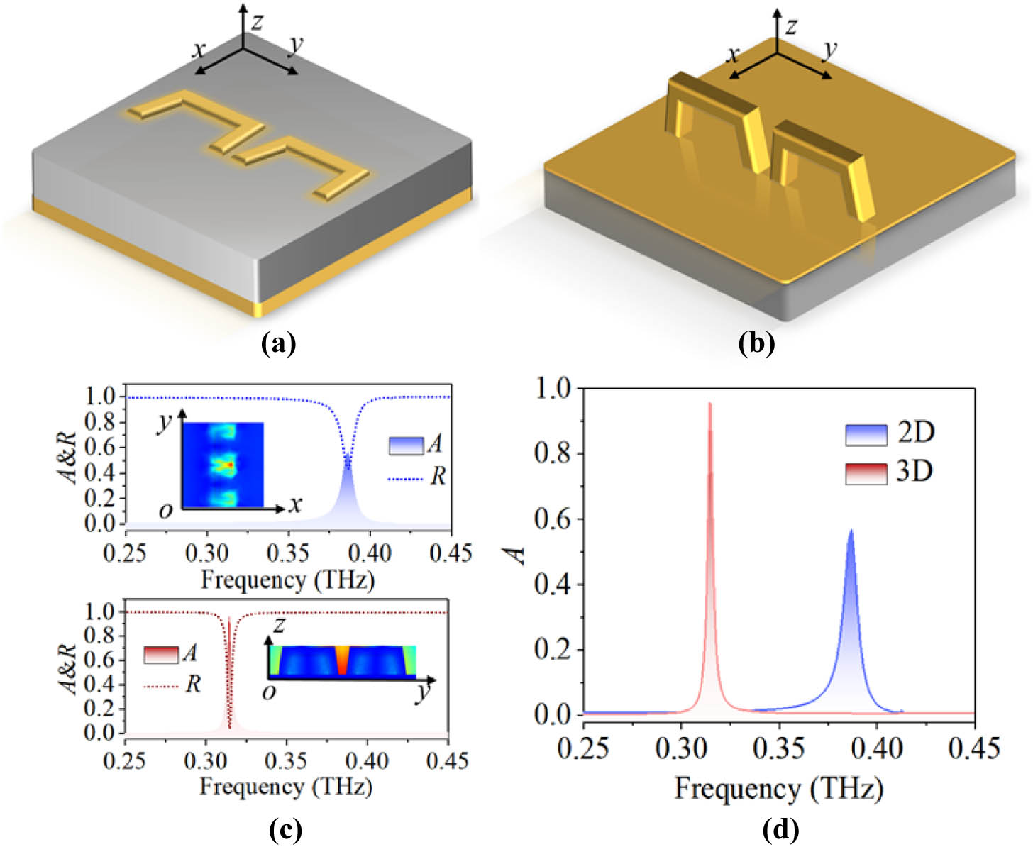
Figure 1.Schematic of (a) metal-insulator-metal 2D meta-absorber and (b) metal-resin 3D meta-absorber. (c) Absorption and reflection spectra of the 2D and 3D metamaterial absorber under
A. Fabrication
Figure 2(a) illustrates the essential steps in manufacturing the proposed absorber with 3D microfabrication by TPP printing and magnetron sputtering. The two-photon absorption and photopolymerization reactions occur only within an extremely small volume, enabling exceptionally high resolution and precision. Initially, the digital model (STL files) is designed by CAD, and read along with 2D images in a GWL editor DeScribe software; the GWL file describes laser focal point trajectories within the resin and sets system parameters for the printing process. Subsequently, the generated parsed GWL files are loaded and scanned in NanoWrite software for errors, and then generate compiled GWLC files for the TPP 3D printing system (Photonic Professional GT2, Nanoscribe GmbH&CO.KG, German) with a laser of 780 nm wavelength in Fig. 2(b). During printing with 100% laser power, the live-view window allows real-time monitoring of the ongoing process. The overall size of the printing area is , containing unit cells. After removing uncured resin with developing solution propylene glycol monomethyl ether acetate and removing developer with the isopropanol, UV light curing is carried out for enhanced structural strength and to prevent structural collapse and a bent beam. These problems in fabrication can also be solved by the following methods. (i) Enhance adhesion to ensure sufficient contact between the printed structure and the substrate surface. The TPP system finds interfaces automatically by detecting changes in refractive indices between two materials of different optical densities along the optical path. is defined as the substrate-resin boundary; we initiate printing from the plane of 0.5 μm below the interface to ensure the mechanical stability of the printed structure. (ii) In order to prevent printing resin parts from drifting away, we employ enough dose for printing the bottom of the column, to ensure the stability of the base. (iii) Employing plasma pre-treatment can increase substrate surface roughness and wettability, thus enhancing adhesion to printing metasurfaces. Finally, we utilized terahertz time-domain spectroscopy (THz-TDS) in the reflection mode to measure the spectra. It emits terahertz-frequency pulse waves to interact with the surface of the sample, partially reflecting back to the detector as in Fig. 2(c).
![]()
Figure 2.(a) Fabrication process of the proposed terahertz meta-absorber. (b) Photograph of TPP 3D printing system. (c) Reflection mode of THz-TDS system.
B. Structural Design
Figure 3(a) represents the arrays of the proposed THz meta-absorber, and the magnified unit cell of gate-frame structured design with copper-coated resin is shown in Fig. 3(b), in which the geometric parameters are set as follows: , , , , , . The copper thickness is typically set as 500 nm, which is slightly greater than the skin depth, ensuring that terahertz waves reduce transmission. The scanning electron microscope (SEM) images of the fabricated metasurface arrays are depicted in Figs. 3(b) and 3(c) with oblique and right top views. It is noted that the three-dimensional structure is arranged neatly along the - and -directions, and the trapezoidal gate-frame structure is designed to be wide at the bottom and narrow on the top, with the purpose of enhancing the overall structural support and strengthening its stability. The magnitude images of unit cells in the top right insets illustrate the complete three-dimensional form, which is consistent with our designed structure. The beam does not collapse even when it reaches 160 μm in length, demonstrating its robust structure.
![]()
Figure 3.(a) Schematic of the metal-resin 3D metasurface of arrays. (b) Geometry of the metasurface unit cell structure. Scanning electron microscope (SEM) images of the fabricated metasurface arrays with (c) oblique and (d) top views.
Additionally, in order to further reveal the structure profile in detail, the images of 3D-printed unit cells from the laser scanning confocal microscope (LSCM) are displayed in Fig. 4(a). Here, the surface height information is provided, by utilizing laser interference patterns formed from the interference between reflected laser light and a reference beam. There are serrated rough edges on the structure surface and vertical stripes on the side of the structure as in Fig. 4(b), which are caused by the low voxels density due to large hatching distances. It is well known that the smaller voxel sizes provide more printing details and higher resolution, but also take more printing time, which is unexpected especially in large-area metamaterial printing. Choosing larger voxel sizes can speed up the printing process and might sacrifice some detail and resolution. Therefore, when selecting voxel sizes, a trade-off should be made among printing speed, resolution, and required detail to determine the most suitable objective lens. Here, the roughness has negligible impact on the absorbance. Hence, to expedite the printing speed, we use larger voxel slicing during resin printing. Along the -direction and -direction, cross-section profiles of the proposed meta-absorber are extracted as in Figs. 4(c) and 4(d), in which the height and width are around 81.5 and 31 μm, further affirming the reliability and accuracy of the printing process.
![]()
Figure 4.(a) Images of 3D-printed unit cell from the laser scanning confocal microscope (LSCM). (b) SEM image of rough edges on the structure surface. Cross-section profiles of the proposed meta-absorber along the (c)
C. Simulated Results
To obtain the absorption rate and extract the -parameter in the numerical simulations, COMSOL Multiphysics is employed by a finite element method (FEM) for electromagnetic analysis. Here, periodic boundary conditions were set along the unit cell of - and -directions to form arrays, and an open boundary is set along the -axis. Additionally, the absorber is analyzed under normally -polarized and -polarized incident waves. The absorption rate is extracted by the formula ; the -parameter of the proposed meta-absorber comprehensively can be obtained directly in COMSOL Multiphysics. Here, the transmittance is approximately equal to zero because terahertz waves are typically blocked by the surface of a continuous metal reflector, thus unable to penetrate through metal plates. Therefore, the absorptivity can be derived from the reflection coefficient as .
Figure 5(a) illustrates the top view of SEM image of the sample, in which the inset plots are magnified images of a single pattern. The absorptivity and reflectivity under - and -polarizations are compared in Fig. 5(b); it can be seen that the resonance occurs at different frequencies, because the absorption spectrum is polarization-sensitive due to the broken symmetric structure. For -polarization, the resonant absorption peak appears at 0.3142 THz frequency, achieving an almost perfect absorptivity with a full width at half maximum (FWHM) of 3.1 GHz. However, for -polarization, the absorptivity resonance occurs at 0.7808 THz frequency with a maximum absorptivity of 80.7% with an FWHM of 3.1 GHz. For the sensors, both -factor and FWHM reflect the sensing characteristics. A high -factor implies a relatively low influence from non-target signals or external interference, and enhancement to detecting weak biological signals, which is desirable in sensor optimization. Here, the -factor of the meta-absorber is given by , in which represents the absorption resonance frequency, and FWHM represents the width of a spectrum. The -factor for -polarization at 0.3142 THz absorption peak is 104.67, and that of -polarization at 0.7808 THz absorption peak is 251.87, indicating outstanding narrowband absorbing performance. Additionally, polarization sensitivity enables the single device to achieve narrowband absorption in two frequency ranges, increasing application versatility, and avoiding redesign and manufacturing waste.
![]()
Figure 5.(a) SEM image of top view. (b) Absorption and reflection spectra of the meta-absorber under
In order to reveal the physical mechanism of the proposed meta-absorber and validate simulations through a physical analytical model, coupled mode theory (CMT) [23,24] is introduced to explain the absorbing phenomenon. CMT serves to describe the coupling between resonators or ports through the input-output of resonators, and study the absorption or reflection behavior of electromagnetic waves within the resonator. Here, the meta-absorber in this study can be regarded as a single-port resonator, and the reflectance of the absorber can be derived as
Here, and represent the amplitudes of the output and input waves, respectively, is the internal dissipation within the resonator, while is the radiation loss of energy dissipation outward. We can clearly observe the behavior of electromagnetic waves within the device via these parameters, and explore our study of absorption mechanisms. Since the continuous metallic reflector prevents the transmission of electromagnetic waves as mentioned above, the absorption rate is
According to the formula, when the resonance frequency of the absorbance and the intrinsic loss is equal to radiation loss , the reflectance becomes zero; thus the device achieves perfect absorption of incident electromagnetic waves, and the and in Eq. (2) can be determined by curve fitting. It can be seen in Fig. 5(c) that the fitting curve is in good agreement with the simulated curve. Therefore, explaining perfect absorption using CMT has a clear representation of parameters of intrinsic loss and radiation loss associated with a particular resonance mode, and also brings about a better understanding of the behavior of electromagnetic waves within the structure. It provides a better explanation for the inherent mechanisms causing the dissipation of electromagnetic waves.
According to the mentioned formula , to achieve perfect absorption of electromagnetic waves, it is necessary to minimize both the transmission and reflection rates. Lowering the transmission rate of the metamaterial can be realized by employing a continuous metal reflector and configuring a thickness greater than the skin depth at terahertz frequencies to prevent the transmission of electromagnetic waves. Hence, another requirement is to lower the reflectance, by optimizing geometric parameters, which is essentially adjusting equivalent impedance. Impedance matching originally referred to a suitable match between the signal source and the load in microwave electronics, with the purpose of eliminating signal reflection. Here, the concept is induced with the external environment seen as the input and the device as the output [25]. It considers the device as a whole, correlating impedance with reflection rates, thereby simplifying computational steps. The reflection rate of the metamaterial determined by its intrinsic impedance and that of free space is as the following formula:
Here, , which represents the impedance of free space, and denotes the relative impedance of metamaterial to free space. Therefore, is a crucial considered index in absorber design. The closer the impedance values of the two impedances, the lower the reflection and the higher the absorption rate. Actually, adjusting the geometric parameters of the meta-absorber such as the thickness, side length, and periodicity of the metamaterial unit structure can achieve impedance matching. When the impedance , the metamaterial matches the impedance of free space perfectly. At this point, incoming electromagnetic waves enter the metamaterial almost without reflection. They are absorbed by metal losses and converted into thermal energy. Here, based on the simulation-derived -parameter, the metamaterial relative impedance of the absorber can be calculated as the following expression [26,27]:
Figure 5(d) illustrates the effective impedance spectrum derived from the -parameter, in which the solid line and dotted line represent the real part and imaginary part of . The real part of approximately approaches one at 0.314 THz, while the imaginary part tends towards zero. At this point, the absorber achieves good impedance matching with free space. Consequently, the extent of electromagnetic wave penetration into the absorber interior is maximized, leading to the largest dissipation and perfect absorption. Based on the impedance match analysis, it is clear how various geometric parameters of the metamaterial affect the absorbance coefficients, which contributes to a better design and optimization of the structure.
To explain the absorption mechanism from an electromagnetic field perspective, we calculated the electric and magnetic field distributions of resonance under -polarized incident waves at 0.3142 THz and -polarized incident waves at 0.7808 THz. The electric field distribution for -polarization of a top view on the plane in Fig. 6(a) displays the primary resonant mode, in which the electric field mainly concentrates on the upper surface of the crossbeam and reaches up to a maximum intensity enhancement of . From the side view on the plane in Fig. 6(b), the magnetic field primarily is constrained in the gap between adjacent gate-shaped resonators, reaching a maximum magnetic field intensity of . The incident electromagnetic energy effectively is confined to the upper surfaces of the gate-shaped structure and the intervals between adjacent structures, thus realizing perfect absorption. Additionally, for -polarization, the side view on the plane in Fig. 6(c) indicates an extensive electric field distribution on both upper and lower sides of the entire crossbeam, reaching a maximum electric field intensity of . The magnetic field mainly concentrates on the ends of the upper surface on the plane as Fig. 6(d), with a maximum magnetic field intensity of . The absorption is attributed to the resonance excited around the gate-shaped 3D structure, where both electric and magnetic fields are significantly enhanced. The incoming electromagnetic wave energy gets captured and suppressed between the perpendicular columns, preventing wave reflection from the resonator. Unlike conventional 2D plane metamaterial, 3D structures possess the ability to manipulate the electromagnetic field along the -axis in vertical space. This capability enhances the diversity in designing high-performance absorbers with intense localized field enhancement.
![]()
Figure 6.Distributions of the (a) electric field and (b) magnetic field under
According to the analysis of the equivalent impedance, it is known that the resonance is determined indirectly by geometric parameters like the aspect ratio. However, in experiments, 3D printed structures with significantly high aspect ratios might lead to collapse as in Fig. 7(a) due to inadequate adhesion to the substrate. Overextended cantilever beams also lead to the problem of bent beams due to lacking sufficient support, and the drift of voxels during printing. To ensure the stability of the base, the bottom of the column is printed with higher laser power as in Fig. 7(b). Additionally, a high aspect ratio might lead to collapse, so a series of parameter ( and ) sweeps were carried out to investigate the impact of aspect ratios on absorptivity. The aim is to select an appropriate aspect ratio, and ensure the high absorption rate and the non-collapse of fabrication. The results are shown as Figs. 7(c) and 7(d), respectively. At -polarization of normal incidence, when parameter increases from 100 to 140 μm, the resonant absorption frequency has a slight redshift from 0.32 to 0.313 THz while the amplitude remains almost stable. The resonance frequency variations stay within a small range, indicating good stability and tolerance of fabrication, with relatively low dependence on manufacturing precision. Similarly, in Fig. 7(c), when varies from 60 to 80 μm, the frequency of the resonant absorption has a red shift from 0.58 to 0.32 THz. The acceptable impact of reduced height on the reflection spectra offers a viable means to adjust the spectra frequency. Additionally, the absorption performance is highly sensitive to slight variations of the gap of adjacent resonators as in Fig. 7(e). When the gap of adjacent resonators decreased from 20 to 6 μm, the FWHM of the resonance significantly increased and the maximum absorption peak decreased from 1% to 56%. In the experiment, we employed magnetron sputtering to deposit copper on the surface; the beam in the middle of the structure prevents metal deposition inside the structure, and the extremely small spacing between adjacent resonators leads to poor uniformity of the metal film on the trapezoidal sidewalls compared to the flat surface. Here, we simulated the absorption under extreme conditions with no metal deposition on the side, as shown in Fig. 7(f); the absorption attenuates to 49%.
![]()
Figure 7.(a) SEM image of the collapsed structure. (b) SEM image of the column bottom with higher laser power. Absorption spectra of the meta-absorber with (c) parameter
We next investigated the impact of incident angles of -polarization on the absorption. Here, direction of polarization of the terahertz waves is perpendicular to the incident plane , with electric field direction parallel to the -axis. The angle of incidence refers to the angle between the direction of propagation and the normal to the interface as in Fig. 8(a). When electromagnetic waves are obliquely incident in -polarization, the electric field is always along the -axis. With increasing incident angles, the component of the magnetic field at the -axis leads to reduction of the effective projected area. This results in the weakened absorption as in Fig. 8(b). As the incident angle gradually increases from 0° to 64°, the maximum absorption rate slightly decreases from 100% to 89% with a minor blueshift. When the incident angle is beyond 80°, the absorption rate further declines to 57%. The absorbance shows moderate sensitivity to the incident angle; its bandwidth remains relatively stable. Therefore, even with slight oblique incidence due to uneven placement during measurements, the deviation from normal incidence remains negligible.
![]()
Figure 8.(a) Schematic diagram of incident angle of
3. SENSING RESULTS
During THz-TDS measurement, to eliminate the influence from environment, the reflection coefficient can be expressed as a function of normalized reflected THz electric field amplitude between the measured sample and reference gold sample . The time-domain spectra are extracted in Fig. 9(a). Compared with the reference gold sample, the device leads to a reduction in the amplitude of pulse signals and slight phase delay, attributed to the absorption and scattering effects of the metamaterial on terahertz waves. They are converted to frequency-domain spectra via fast Fourier transform (FFT). The measured terahertz spectra of a bare meta-absorber obtained through THz-TDS are depicted in Fig. 9(b), showing good agreement with simulated results. It shows narrow bandwidth characteristics around 0.3143 THz and maximum absorption of 77%, indicating its good absorption characteristics in terahertz range. The measured resonant frequency at 0.3143 THz is close to the simulated result at 0.3142 THz. The failure to reach perfect absorption could be due to electromagnetic wave leakage caused by incomplete metal coverage on the lower surface of the beam. The absorption spectrum maintains high absorption () from 0.274 to 0.357 THz range. Based on past experimental experience, the -factors of measured results tend to be lower than those of simulated results. The small difference of measurement might be caused by manufacturing deviation. On the one hand, the reason for the discrepancy is the resonator drift during the development process as discussed in Fig. 7(e), particularly influenced by the gap of the resonance. On the other hand, during the printing process, inaccurate interface finding between the substrate and the resin would result in a smaller printing height. The impact of geometric parameters on absorption is significant. Both factors of manufacturing deviation would lead to an increased FWHM.
![]()
Figure 9.(a) Reflected TDS signals of metasurface sample and gold reference. (b) Measured absorbance spectra. (c) Calculated absorbance spectra of the analyte with refractive index of 1–1.8. (d) Relative frequency shift of the proposed meta-absorber versus analyte refractive index.
In order to investigate the sensing characteristics of the designed meta-absorber as a refractive index sensor, we calculated the absorption spectra of the analyte with different refractive indices coated on the surface of the sensor. The designed sensor provides specific information on the spectrum, such as resonant frequencies. The absorption spectra are depicted in Fig. 9(c). As the refractive index of the analyte gradually increases from to , the resonant frequency of the proposed meta-absorber has a redshift from 0.3142 to 0.1738 THz uniformly, with frequency shift of 140.4 GHz. This is attributed to the fact that the analyte adheres to the surface of the resonator, increasing the local equivalent dielectric constant of the surrounding medium, thus leading to a noticeable frequency shift. Therefore, the proposed sensor has the capability to detect analytes with varying refractive indices. The resonances with narrow linewidths are admired for accurate sensing. Here, the sensitivity of resonant frequency to the refractive index is induced to assess sensor performance. It is defined as , in which and represent the resonant frequency shift and refractive index change, respectively. Another parameter used to estimate sensing performance is the figure of merit (FOM), expressed as . Here, the relationship between the resonance frequency and the refractive index of the analyte is extracted in Fig. 9(d) to show the relative frequency shift clearly. It is observed that the resonance absorption frequency shows a linear shift monotonically, with the fitted lines as , in which the slope represents sensitivity. Therefore, the proposed meta-absorber exhibits a sensitivity of 172.5 GHz/RIU, with FOM of 19.56.
Here, we compare the proposed meta-absorber with recently reported refractive index meta-absorbers, as shown in Table 1 to provide a clearer understanding of the sensing performance. Obviously, compared with traditional in-plane metasurface with plasmon and all-dielectric, the proposed out-of-plane 3D meta-absorber has the advantages of high -factor, narrow band width, and simple fabrication process, and it shows remarkable sensitivity to the refractive index. Compared with traditional lithography processes, TPP 3D printing greatly increases the flexibility of design while ensuring high accuracy. In summary, it meets the requirements of a simple design for a vertical metasuface and is an excellent sensing platform for biochemical detection. Comparison with Other Meta-absorbersRef. Structure Material Sensitivity Fabrication Target analyte [ Inverted-cross-star (ICS) structure Cu 69.8 1.18 GHz/RIU — — [ Square ring and four T-shaped strips Au/Si 202.3/121.4 37 GHz/RIU Electron beam lithography (EBL) — [ Two opposing T-shaped pillars Si — Photolithography and deep reactive ion etching Bt protein [ Cylinder and ring Si 20.6 0.5 and 0.87 THz/RIU Photolithography and deep reactive ion etching Liquid paraffin, gasoline, ethanol, and cancer cell [ Dual copper semitoroidal structure Cu 20 52.5 GHz/RIU Wet etching Ethanol and sucrose solutions
In the following measurement of sensing performance of the proposed terahertz meta-absorber, we have extracted a series of absorption spectra with different amounts of DCH. Doxycycline is an antibiotic widely used as a food preservative and drug to treat diseases in farm animals, but antibiotics abuse can lead to drug resistance, and long-term overuse can lead to doxycycline residues in food, which poses potential harm to both human health and environments. Therefore, accurate detection of trace amounts of doxycycline is essential to ensure food safety, as well as to prevent the potential risks of drug residues. Here, during the pre-treatment, DCH solutions of various concentrations (ranging from 0 to 4 mg/mL) were dropped onto the resonator surface, and then the sample was placed in a nitrogen-dried environment to avoid the influence of water vapor on measurement. The DCH disturbs the surface dielectric environment especially in the gaps of resonators, resulting in changes in the absorption spectrum. The measured results depicted in Fig. 10(a) indicate a remarkable monotonical decrease of the absorption peak, and exhibit an obvious redshift with the increase of concentrations. The inset provides details of an enlarged view of the spectrum. The increase of DCH concentration on the sample prevents the interaction between the electromagnetic waves and the 3D metallic resonance, weakening the excited electric field strength. Consequently, the absorption peak-valley difference decreases. In order to represent the spectrum characteristic parameters clearly, we extracted the responding absorption peaks and their resonance frequencies for analysis as in Figs. 10(b) and 10(c). With the rise in DCH concentration from 0 to 4 mg/mL, the absorption intensity decreases around 49% (from 78% to 29%), with the resonant frequency shift around 70 GHz (from 0.32 to 0.25 THz), which exhibits the high sensitivity of the metasurface to the surrounding dielectric environment.
![]()
Figure 10.(a) Measurements of absorbance spectra of DCH with solution concentrations of 0.1 mg/mL, 0.5 mg/mL, 1 mg/mL, 2 mg/mL, 4 mg/mL. (b) Extracted results and (c) contour map between DCH solution concentrations and peak intensity as well as peak frequency.
4. CONCLUSION
In this work, a 3D meta-absorber with perfect absorbance and prominent -factor of 104.67 has been proposed. Besides, the meta-absorber can be used as a sensor with theoretical sensitivity to refractive index of 172.5 GHz/RIU and FOM of 19.56. Here, using non-photolithographic TPP 3D printing technology, we have successfully manufactured beams with lengths up to 140 μm. Compared with traditional absorber fabrication, these manufacturing steps are flexible, low-cost, and require only two steps. And the measured absorbance agrees well with the simulated results. Furthermore, we have experimentally demonstrated the feasibility of utilizing a 3D terahertz metasurface as a platform for trace DCH sensing. In summary, the TPP 3D manufacturing strategies are highly precise, easily extending to optical devices with smaller scales, and the proposed narrowband meta-absorber has great potential in sensing applications.
References

Set citation alerts for the article
Please enter your email address
© Copyright 2018-2021 | Chinese Laser Press. All Rights Reserved 沪ICP备15018463号-20