
Carlos A. Ríos Ocampo. In-situ nonvolatile and volatile modulation for optical neural networks[J]. Advanced Photonics, 2023, 5(5): 050501
- Advanced Photonics
- Vol. 5, Issue 5, 050501 (2023)
Abstract
High-performance integrated optical memristors are crucial in developing optical neural networks based on in-memory computing. Such devices are building blocks capable of modulating the transmission of a propagating mode in a multilevel and nonvolatile fashion, thus allowing storage and multiplication of analog signals in the same device.1 Chalcogenide phase change materials (PCMs) are candidates for high-performance devices. They display sought-after nonvolatile states with large optical contrast and the capability of achieving intermediate levels via spatial and temporal distributions of amorphous and crystalline domains. Both phase and amplitude modulation are possible with PCMs depending on the alloy of choice; for instance, and have gained space as phase shifters, while (GST) has been employed as amplitude modulators in the C-L bands. The choice of photonic device naturally follows the selection of PCM. While GST is deposited directly on top of a straight waveguide to modulate amplitude, and require a resonator to achieve amplitude modulation via phase tuning; typically, a microring resonator.
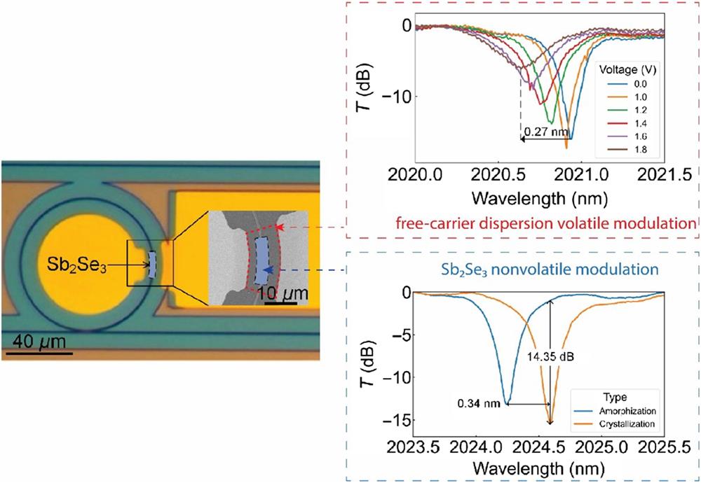
At the device level, the challenge is to switch PCMs between the amorphous and crystalline states in a controlled manner with high cyclability and level repeatability. The switching is triggered by alloy-specific thermal stimuli, which generally require annealing for crystallization and melt-quenching for amorphization. These thermal stimuli on photonic integrated circuits (PICs) were initially demonstrated using optical approaches,2 but recently, electro-thermal switching employing on-chip microheaters has become more relevant thanks to better integration and scalability.3,4 Since built-in doped-silicon microheaters are well known in PICs, the phase change photonics community quickly adopted them as the ideal, scalable, and foundry-compatible platform to switch PCMs. However, such devices have served as amplitude or phase modulators that exploit only the nonvolatility property. Now, M. Wei and colleagues have demonstrated a PIC building block comprising a microring resonator with embedded doped-silicon p-i-n diode and a cell that can undergo volatile and nonvolatile electrically driven modulations.5 The nonvolatile modulation is achieved by controlling the phase transition of via electro-thermal induced Joule heating. The volatile sub-microsecond modulation is achieved via free-carrier dispersion by forward biasing the diode, which, crucially, is operated so the device’s temperature remains below the crystallization temperature of . To achieve this performance, and contrary to more traditional amplitude modulation of alloys such as GST for optical computing,6,7 the team chose the phase modulation of in a microring resonator because this approach also enables exploiting the volatile phase shift induced by the free-carrier dispersion (see Fig. 1).
![]()
Figure 1.Silicon-on-insulator photonic integrated circuit with embedded p-i-n microheater and
Dual volatile and nonvolatile modulation has been proposed before;8,9 however, Wei et al. show the first application of both mechanisms in optical neural networks (ONNs) and cleverly use them in a multi-functional device for storage, computing, and in-situ training—unprecedented versatility in a single PIC building block. In particular, the ONN comprises microring resonator arrays and wavelength division multiplexing to perform matrix-vector multiplications, and they refer to in-situ training as the tuning of the ONN to achieve optimal performance, which is done directly in the optical domain via volatile tuning of the microrings’ response. Once ONN achieves the expected output, the trained weights are written into the PCM memories for nonvolatile storage. This innovative approach improves the training speed and compensates for manufacturing errors and crosstalk. Outstandingly, the maturity of the fabrication achieved by Wei et al. is critical to attaining 5-bit (32 levels) storage—which also determines the precision of the computation—with repeatable switching and CMOS-compatible voltages.
Sign up for Advanced Photonics TOC. Get the latest issue of Advanced Photonics delivered right to you!Sign up now
While shown at the device level, the co-located volatile and nonvolatile modulation provides a feasible solution to constructing large-scale ONNs based on optical memristors with in-situ training capability. To reveal the full potential of this multifunctional device, the experimental demonstration of an architecture is the next natural step. This is an exciting prospect for photonics but also a big challenge on several fronts, such as integrating PCM to foundry processes, demonstrating high fabrication yield, achieving multilevel control in a repeatable manner (the 5-bits claim is not yet demonstrated with high cyclability), finding PCM alloys with larger optical contrast and lower switching energy, among others. These are open challenges that make the fast-growing field of phase-change photonics a vibrant new field worth watching closely.
Carlos A. Ríos Ocampo (aka Carlos Ríos) is an assistant professor at the University of Maryland (UMD), College Park, Maryland, USA, where in 2021 he established the Photonic Materials and Devices group. He received a BS degree in physics from the University of Antioquia, Colombia; an MSc degree from the Karlsruhe Institute of Technology, Germany; and a PhD degree from the University of Oxford, UK. Prior to joining UMD, he was a postdoctoral associate with MIT between 2018 and 2021. His research interests include photonic and phase-change materials, nanoscale light-matter interactions, photonic integrated circuits, and photonic (neuromorphic) computing.

Set citation alerts for the article
Please enter your email address
© Copyright 2018-2021 | Chinese Laser Press. All Rights Reserved 沪ICP备15018463号-20