An out-of-plane silicon grating coupler capable of mode-order conversion at the chip–fiber interface is designed and fabricated. Optimization of the structure is performed through finite-difference time-domain simulations, and the final device is characterized through far-field profile and transmission measurements. A coupling loss of 3.1 dB to a commercial two-mode fiber is measured for a single mode conversion grating, which includes a conversion penalty of 1.3 dB. Far-field patterns of the excited mode profile are also reported.
1. INTRODUCTION
The increasing demand for capacity in modern networks has brought space-division multiplexing (SDM) to the forefront of current research on optical communications [1,2]. Among the different implementations of SDM, the use of multi-mode fibers has emerged as a highly attractive solution to augment the amount of information carried by a single fiber by means of allocating distinct data streams to different modes [3]. In the meantime, silicon photonics is widely used in communications applications, offering a cost-effective route to the implementation of high-performance integrated devices. The introduction of two basic building blocks is essential in applications that require the combination of silicon photonics with few-mode fiber (FMF) technology: an efficient FMF-to-silicon-on-insulator (SOI) interface and an integrated mode multiplexer. Of these, FMF-to-SOI interfaces can be realized by means of an appropriately large grating coupler as shown in Refs. [4,5]. Mode multiplexing on a purely integrated level has also been reported through either the use of multimode waveguides [6–8] or a technique that transfers part of the mode conversion operation to the waveguide-fiber interface using electro-optic phase shifters and multiple small-scale gratings appropriately positioned to illuminate different spots of the comparatively larger FMF cross section and thus excite higher-order linearly polarized (LP) modes [9–12].
Mode-order conversion represents the fundamental functionality required for such mode multiplexers. In this paper, we report the design and characterization of the first, to our knowledge, fabricated grating coupler capable of converting the waveguide mode to the mode of a two-mode fiber solely owing to its pattern design, with no additional phase shifter components [13]. This design approach implements the mode conversion functionality entirely at the FMF-to-SOI coupling stage and focuses on optimizing the efficiency of the conversion process as well as the coupling efficiency. A similar design route was discussed through simulations in Ref. [14], though no experimental verification was presented. For the grating pattern described in this paper, the design strategy and simulation results are first presented, with a discussion on the coupling efficiency and the conversion penalty. We then discuss the experimental results obtained by characterizing the fabricated SOI devices.
2. DESIGN AND SIMULATION
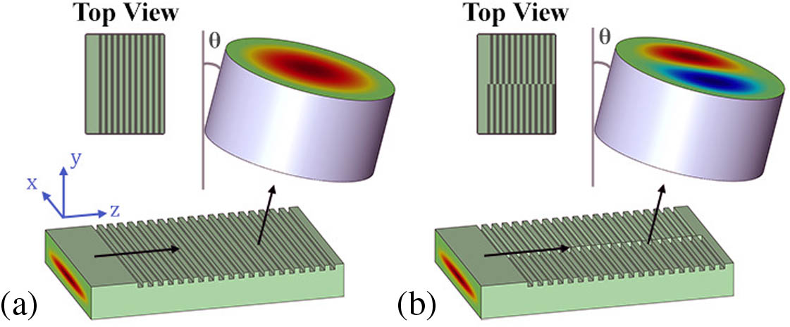
The operation of out-of-plane grating couplers (GCs) relies on phase matching between the waves propagating in the waveguide and those propagating in the coupled fiber (Fig. 1). The couplers comprise an array of individual scatterers arranged in a way to ensure that the phase characteristics of an in-plane wave are modified to produce an out-scattered wave propagating at an angle. The scatterer distribution on the chip plane is determined by the phase-matching condition, which is described by the equation , where and express the spatial phase distributions of the fiber mode and the in-plane mode propagating along the grating part of the waveguide, respectively, for the area spanning the surface of the silicon chip (the plane in Fig. 1). A structure that incorporates an additional mode-order conversion operation satisfies the same principle, with the phase functions corresponding to those of the desired waveguide–fiber mode pair. Hence, converters to any higher-order fiber mode can be designed following this principle [14,15]. In the specific case of a mode conversion, the solution to this equation is described by the pattern illustrated in Fig. 1(b), where the grooves on one side of the grating are offset with respect to the other side by a half-cycle of their spatial frequency. This effectively creates a phase difference along the direction of the mode profile, which matches the phase function of an fiber mode. (Note that this discussion also applies to the reciprocal operation, i.e., the coupling of a certain fiber mode to a waveguide mode.)
Sign up for Photonics Research TOC. Get the latest issue of Photonics Research delivered right to you!Sign up now
Figure 1.3D concept of the grating-fiber interface for (a) a regular grating pattern and (b) a mode-converting grating pattern (dimensions not to scale). Insets: top view of the gratings.
Besides matching the phase profile of the mode, the out-scattered light must also match its Gaussian intensity profile to achieve a high coupling efficiency. Therefore, the design of the grating coupler described in this paper comprises two distinct steps: (i) grating apodization to optimize the waveguide-fiber coupling efficiency (intensity profile matching) and (ii) offset positioning of the grating teeth to convert the mode order (phase profile matching).
A. Apodization Technique
The first step in our design involved the optimization of a regular grating pattern () in terms of its coupling efficiency to an optical fiber. To achieve this, the 2D structure illustrated in Fig. 2(a) was simulated with the finite-difference time-domain (FDTD) method using the FDTD Solutions software by Lumerical Inc. This structure represents part of the side view ( plane) of a grating coupler with 22 grooves written on a 220-nm-thick silicon wafer, which was selected to enable guiding of TE modes at 1550 nm and was designed to match the wafers available for fabrication. The surroundings of the silicon layer were also included in the simulation, namely, a 2-μm-thick buried oxide (BOX) layer and a 720-nm-thick cladding, both made of , as well as the silicon substrate underneath the BOX layer. To evaluate the coupling efficiency of the simulated grating, a Gaussian beam input was used to represent an optical fiber mode incident on the structure. Its waist was selected to be 20 μm, which corresponded to the mode field diameter (MFD) of a commercial two-mode fiber, and it was launched at a 14.5° angle to the grating to ensure unidirectional propagation in the waveguide. The power coupled into the chip was then monitored after 10 μm of propagation along the waveguide at its cross section on the plane.
Figure 2.(a) Side view of the first four grooves of an apodized grating ( layer thicknesses not to scale), (b) contour plot of the maximum coupling efficiency with respect to the etching depth and the linear apodization factor R.
As illustrated in Fig. 2(a), the periodicity in the groove pattern of the grating was set to vary along its length in order to improve the coupling efficiency to/from an optical fiber. This is because a uniform pattern with identical teeth across its length introduces high coupling loss as a result of the low overlap between the fiber mode and the grating mode. Hence, in order to achieve high coupling efficiency, we have applied a linear apodization to the filling factor and the period of the grating grooves [Fig. 2(a)] as described in Ref. [16]. This enables the grating to optimally couple to/from Gaussian-shaped fiber mode profiles as well as to maintain its directionality across all scatterers. The filling factor for each radiative unit of length is defined as the ratio of the length of the unetched part over the groove period , and its linear apodization is described by the equation where is the filling factor at an arbitrary position , is the filling factor used in the first groove, and expresses the linear apodization factor. For the aforementioned structure parameters as well as the Gaussian beam input, a campaign of 2D FDTD simulations was run on the plane by sweeping the apodization factor and etching depth, resulting in the contour plot shown in Fig. 2(b). The results indicated an optimum coupling efficiency of 68% for an apodization factor of μ and an etching depth of 110 nm. To evaluate the improvement offered by the apodization technique, a uniform grating was simulated in the same environment, and its maximum achievable coupling efficiency was calculated to be 57%, which suggests a gain of 0.76 dB through the use of apodization. The contour plot also shows the robustness of the apodization design, indicating that the efficiency does not change by more than 4% for etching depth and apodization factor margins of and μ, respectively.
B. Groove Positioning for Mode-Order Conversion
Next, based on the optimum configuration for apodization and etching depth, we created a 3D model of the grating coupler that had a width of 20 μm for the purpose of spot size matching and on which we additionally introduced the offset in the groove positioning to realize the mode conversion operation. Therefore, the pattern produced by optimizing the apodization in Section 2.A above was used in one part of the grating [the right-hand side (RHS) in Fig. 3(a)], while the second part consisted of scatterers positioned at an appropriate offset relative to the first part [left-hand side (LHS) in Fig. 3(a)]. This offset was calculated individually for each radiative unit of the apodized structure and corresponded to half of its period, since it was required to introduce a phase delay to the radiated electric field. Bragg’s law can be recalled in order to justify the value of this offset. In a grating coupler radiating at an angle [Fig. 3(b)], the phase delay experienced by the wave propagating in-plane between two successive scatterers and the phase delay acquired by the wave diffracted upwards by the first scatterer have to exhibit a difference of . This is expressed by the following condition: In this equation, represents the vacuum wavenumber, is the effective refractive index of the mode propagating in the grating structure, is the refractive index of the air, is the grating period (radiative unit length), and the angle of radiation in the air (for either cladded or uncladded silicon layers). This results in where represents the coupling wavelength, was considered to be equal to 1, and the value of for each radiative unit is expressed as , where and are the effective indices of its unetched and etched sections, respectively [16].
Figure 3.(a) Top view of the middle area of the mode-converting grating, where the right-hand side and left-hand side patterns meet. (b), (c) Schematic representation of Bragg’s law used to calculate the offset that creates a phase shift of .
Now, the position of a scattering point that results in a -shifted radiated field towards the same angle [Fig. 3(c)] can be found by solving the equation In this equation, represents the distance of the desired scattering point from the reference point [Fig. 3(c)]. This results in , meaning that trenches should be positioned at the middle point of each radiative unit in order to introduce a phase shift to the radiated light [indicated by the blue points in the schematic of Fig. 3(a)]. Thus, this positioning was implemented to the LHS pattern as shown in the top view of the mode-converting grating in Fig. 3(a). Considering that the RHS was apodized according to the method described in Ref. [16], it consisted of a set of periods and , and therefore the LHS trenches were positioned at and formed the LHS set of periods [Fig. 3(a)]. The filling factor of these LHS scatterers was then also apodized appropriately to maintain the same directionality.
The end result for the two sides of the grating is given in Table 1, which lists the positions and sizes of each trench along the axis of the chip. Three-dimensional FDTD simulations were performed on the final design to calculate its coupling efficiency by means of launching an beam to the grating and measuring the power coupled into the waveguide. The coupling efficiency with respect to wavelength is plotted in Fig. 4(a) along with that of a regular () apodized grating coupler for comparison. The plots show maximum efficiencies of 68.4% () and 55.6% () for the regular and mode-converting grating, respectively, which seem to slightly surpass the coupling efficiencies reported in Ref. [14], where maximum values of 60.4% () and 51.5% () were reported. An conversion penalty of 0.9 dB is observed at the peak wavelength, which is attributed to a fraction of the mode power being incident on the discontinuity in the middle of the grating and thus experiencing refraction downwards to the bottom oxide layer and not coupling into the waveguide. To also verify the functionality of the grating for the reverse conversion operation, a simulation was run for a waveguide mode input, out-scattering to a converted profile, which can then be onward coupled to a fiber mode. The intensity profile measured above the grating exhibits two distinct lobes as illustrated in Fig. 4(b). The figure also includes a phase plot for the component of the electric field , which confirms the phase difference between the two lobes. In order to also evaluate the amount of backreflection, the fraction of power propagating in the waveguide towards the opposite direction was monitored, showing a low value of 1.2%.
Figure 4.(a) Simulated coupling efficiency for a regular and a mode-converting grating coupler, (b) intensity profile at the output plane above the grating and phase profile at μ after conversion of to out-of-plane (compatible with ).
To experimentally verify the functionality of the grating coupler, the design was fabricated on an SOI wafer with a 220-nm-thick silicon layer over 2 μm of buried . The pattern was defined by means of electron beam lithography and inductively coupled plasma (ICP) etching, while a 730-nm-thick layer of was subsequently deposited on top of the silicon layout [see Fig. 5(a)]. To characterize our device, we measured the output far-field patterns and the fiber-to-fiber transmission on two types of test waveguides with grating input and output interfaces as shown in Figs. 5(b) and 5(c). The first waveguide comprised only regular apodized grating couplers, while the second one implemented the mode conversion on the output grating. As illustrated in the schematics in Figs. 5(b) and 5(c), the optical input to the waveguides was coupled through a single-mode polarization-maintaining (PM) fiber positioned above the surface of the input grating pattern, while the output was collected on the other end by an infrared (IR) camera through an objective lens placed at an angle above the output grating. A wavelength-tunable external cavity laser source was used to launch TE polarized light (comprising only the component) to the waveguide through the PM fiber at the input and the resulting far field patterns for the two devices are shown in Figs. 5(b) and 5(c), as captured by the camera.
Figure 5.(a) Scanning electron microscope (SEM) image of the mode-converting grating (top view), (b), (c) characterization setup and recorded output far-field patterns for waveguides interfaced with a pair of regular gratings and a regular and a mode-converting grating.
For the first device, which did not involve any mode conversion stage, it can be observed that the output beam shows a -shaped profile with a single intensity lobe. In the second device however, mode-order conversion takes place at the output grating coupler, transforming the waveguide mode to a mode profile resembling the mode (which can be coupled to an fiber mode), as is evident by the two intensity lobes at the output. In order to determine the purity of the converted -shaped pattern, the power profile along the horizontal line that bisects the mode is also plotted in Fig. 5(c). An ideal shape would exhibit zero power between the two lobes, and therefore we quantified the purity by measuring the maximum to minimum intensity ratio, which was equal to 8.6 dB.
In order to quantify the coupling efficiency and the mode conversion penalty of the grating, we subsequently coupled the light from each waveguide to a 1-m-long commercial graded-index two-mode fiber. Figure 6(a) shows the fiber-to-fiber transmission response for the device that included the mode-order converting grating, as it was recorded by sweeping the input wavelength. The graph is plotted with respect to launched power, and includes the coupling losses of both the regular grating and the mode-converting one. The peak power was measured at at the wavelength of 1537 nm, and the 3-dB bandwidth of the structure was 42 nm. To confirm the excitation of the mode, we measured the far-field pattern at the output end of the fiber, which exhibited two clearly separated intensity lobes [Fig. 6(a) inset]. The measured peak-to-trough intensity ratio of the fiber mode was 13.8 dB, suggesting a higher modal purity than what was measured at the grating output. Using an additional reference transmission measurement of the regular grating device [by means of the structure shown in Fig. 5(b)], the coupling efficiency for a single mode-converting grating was then extracted and is shown in Fig. 6(b) along with the prediction from the simulation. The measurement appears to match well the simulation result. The peak efficiency is compared to the predicted value of , both exhibited at the central wavelength of 1540 nm. The difference in the two values can be attributed to additional unaccounted losses present in the measurement system. Regarding the bandwidth of the single mode-converting grating, it was calculated to be 51 nm, which is close to the predicted value of 47 nm evaluated in the simulation run. The conversion penalty predicted by the simulations is also confirmed by the experimental results as the extracted peak efficiency for the regular grating coupler (not shown in the graphs) is at 1535 nm, just 1.3 dB higher than the peak value of the mode converter.
Figure 6.(a) Fiber-to-fiber transmission for the mode-converting device (inset: far-field pattern at the output of the two-mode fiber), (b) extracted (and simulated) coupling efficiency for the mode-converting grating coupler.
We have presented a design strategy for grating couplers that implement mode-order conversion at the fiber-chip interface with no requirement for additional components and we have demonstrated the first successful fabrication and characterization of such a structure. The design optimization focused on maximizing the coupling efficiency as well as the conversion efficiency, while the methodology provides scalability to the converter design, enabling potential conversion to any higher-order fiber mode through the use of the appropriate groove pattern (see e.g., Refs. [14,15]). The conversion of a mode to an out-of-plane mode profile was verified through the visualization of the far-field intensity profile radiating from the output of the device, which exhibited two clearly separated lobes. Finally, a conversion was also confirmed by coupling to a two-mode fiber and recording the mode profile at the fiber output, while transmission measurements showed a 3.1 dB coupling efficiency for a single mode-order converting grating, which included a 1.3 dB penalty for the conversion operation.
Acknowledgment
Acknowledgment. D. J. Thomson acknowledges funding from the Royal Society for his University Research Fellowship. The data for this work is accessible through the University of Southampton Institutional Research Repository: https://doi.org/10.5258/SOTON/D0893.
[7] B. Stern, M. Lipson. High-bandwidth link with single laser input using silicon modulators and mode multiplexing. CLEO: Science and Innovations, STu4G-5(2016).
[8] X. Wu, K. Xu, C. Huang, C. Shu, H. K. Tsang. Mode division multiplexed 3 × 28 gbit/s on-chip photonic interconnects. CLEO: Science and Innovations, STu4G-6(2016).
[9] A. M. J. Koonen, H. S. Chen, H. P. A. Van Den Boom, O. Raz. Silicon photonic integrated mode multiplexer. IEEE Photonics Society Summer Topical Meeting Series PSST, 240-241(2012).
[10] N. K. Fontaine, C. R. Doerr, M. A. Mestre, R. Ryf, P. Winzer, L. Buhl, Y. Sun, X. Jiang, R. Lingle. Space-division multiplexing and all-optical MIMO demultiplexing using a photonic integrated circuit. National Fiber Optic Engineers Conference, PDP5B.1(2012).
[12] C. R. Doerr, N. Fontaine, M. Hirano, T. Sasaki, L. Buhl, P. Winzer. Silicon photonic integrated circuit for coupling to a ring-core multimode fiber for space-division multiplexing. European Conference and Exhibition on Optical Communication, Th.13.A.3(2011).
[13] I. Demirtzioglou, C. Lacava, A. Shakoor, A. Khokhar, Y. Jung, D. J. Thomson, P. Petropoulos. Silicon grating coupler for mode order conversion. Conference on Lasers and Electro-Optics, JTh2A.74(2019).