Yuhua Li, Kun Zhu, Zhe Kang, Wai Lok Ho, Roy Davidson, Chao Lu, Brent E. Little, Sai Tak Chu, "CMOS-compatible high-index doped silica waveguide with an embedded silicon-nanocrystal strip for all-optical analog-to-digital conversion," Photonics Res. 7, 1200 (2019)
Copy Citation Text
Passive all-optical signal processors that overcome the electronic bottleneck can potentially be the enabling components for the next-generation high-speed and lower power consumption systems. Here, we propose and experimentally demonstrate a CMOS-compatible waveguide and its application to the all-optical analog-to-digital converter (ADC) under the nonlinear spectral splitting and filtering scheme. As the key component of the proposed ADC, a 50 cm long high-index doped silica glass spiral waveguide is composed of a thin silicon-nanocrystal (Si-nc) layer embedded in the core center for enhanced nonlinearity. The device simultaneously possesses low loss (0.16 dB/cm at 1550 nm), large nonlinearity ( at 1550 nm), and negligible nonlinear absorption. A 2-bit ADC basic unit is achieved when pumped by the proposed waveguide structure at the telecom band and without any additional amplification. Simulation results that are consistent with the experimental ones are also demonstrated, which further confirm the feasibility of the proposed scheme for larger quantization resolution. This demonstrated approach enables a fully monolithic solution for all-optical ADC in the future, which can digitize broadband optical signals directly at low power consumption. This has great potential on the applications of high-speed optical communications, networks, and signal processing systems.
1. INTRODUCTION
As the key front-end signal processors, analog-to-digital converters (ADCs) bridge between the analog and digital worlds and play an important role in modern electronic communication and information systems. Nowadays ADCs with higher speed, larger bandwidth, and better performance are critical components in various advanced systems, such as high-speed optical communication systems, ultra-broadband wireless systems, advanced radar systems, and real-time signal acquiring and processing systems [1,2] that require high-speed digitization of the input signal. The traditional electrical ADCs are limited in these applications when operating at very high frequencies due to their inherent aperture jitter and comparator ambiguity. Photonic ADCs that utilize ultra-low jitter and short mode-locked pulses as the sampling source can digitize the signal in the optical domain, which can solve the electronic bottleneck issues and the approach has been shown to be a promising technology for future ultra-high-speed ADCs [3–6]. In the past two decades, we have witnessed a tremendous effort in the development of all-optical ADCs. These include time-stretching [7,8] or time-interleaving [6,9] techniques that combine with low-speed electronic ADCs, phase-shifted optical quantization techniques [10,11], and all-optical approaches that utilize nonlinear optical effects [12–19]. The former two methods sample the electronic analog signals through electro-optic modulation, where both of them still rely on active devices in the whole digitization process. Hence, the performances of these methods are limited by the bandwidths of the electro-optic modulators. In contrast, the latter nonlinearity-based all-optical ADCs are fully passive in their key modules, i.e., the sampling, quantizing, and coding modules, which can directly digitize broadband optical analog signals in the optical domain without the associated bandwidth limitation from the electronic components. Also, the response time of processing can be up to femtoseconds level. For example, cross-phase modulation (XPM) [20,21] and four-wave-mixing (FWM) [22,23] effects have been used for all-optical sampling from several to hundreds of gigahertz sampling rates. Soliton self-frequency shift [12–15], XPM [16], and self-phase modulation (SPM) [17] effects have been used for all-optical quantization. However, most of the reported nonlinearity-based schemes still require bulky and discrete fiber devices as the nonlinear media of the key sampling and quantizing modules, which only demonstrate the feasibility of the functionalities rather than an expecting prospect of compact form and monolithical integration. Moreover, in order to remedy the weak nonlinear interaction in these silica media, relatively high optical input power or much longer optical fiber must be used, which increases the power consumption of the system along with increases in cost. Recently, the all-optical ADC schemes based on nonlinear waveguides have been proposed showing the feasibility of CMOS-compatible on-chip all-optical ADCs with low power consumption [24–26], but have not been realized.
In this paper, we propose and experimentally demonstrate a newly developed nonlinearity-enhanced waveguide, with which a 2-bit quantization is realized based on the SPM effect leading to a full all-optical ADC operation. The high-index doped silica glass waveguide has a thin silicon-nanocrystal (Si-nc) layer embedded in the middle of the waveguide core that provides a threefold nonlinearity enhancement compared to the waveguide without the Si-nc strip, where the nonlinear coefficient is 20 to 100 times higher than the highly nonlinear fiber (HNLF) or dispersion-shift fiber (DSF) used in the previous studies [14,17,18]. The waveguide is fully CMOS-compatible, and the fabrication process is compatible with other integrated optical components. We investigated both the linear and nonlinear characteristics of the proposed high-index doped silica waveguide with Si-nc strip to evaluate the nonlinearity enhancement effects. For the all-optical ADC operation, the quantization of the optical sampled pulses is achieved at low power level by filtering the broadened and split optical spectrum that is induced by the SPM effect in the proposed waveguide. Experimental and simulation results are demonstrated and show the performances of the proposed 2-bit quantizer for ADC operation. To the best of our knowledge, this is the first experimental demonstration of the CMOS-compatible nonlinear waveguide for all-optical ADC family, showing the proposed ADC as a promising platform in the future high-speed and ultra-broadband digitizing systems.
2. PRINCIPLE
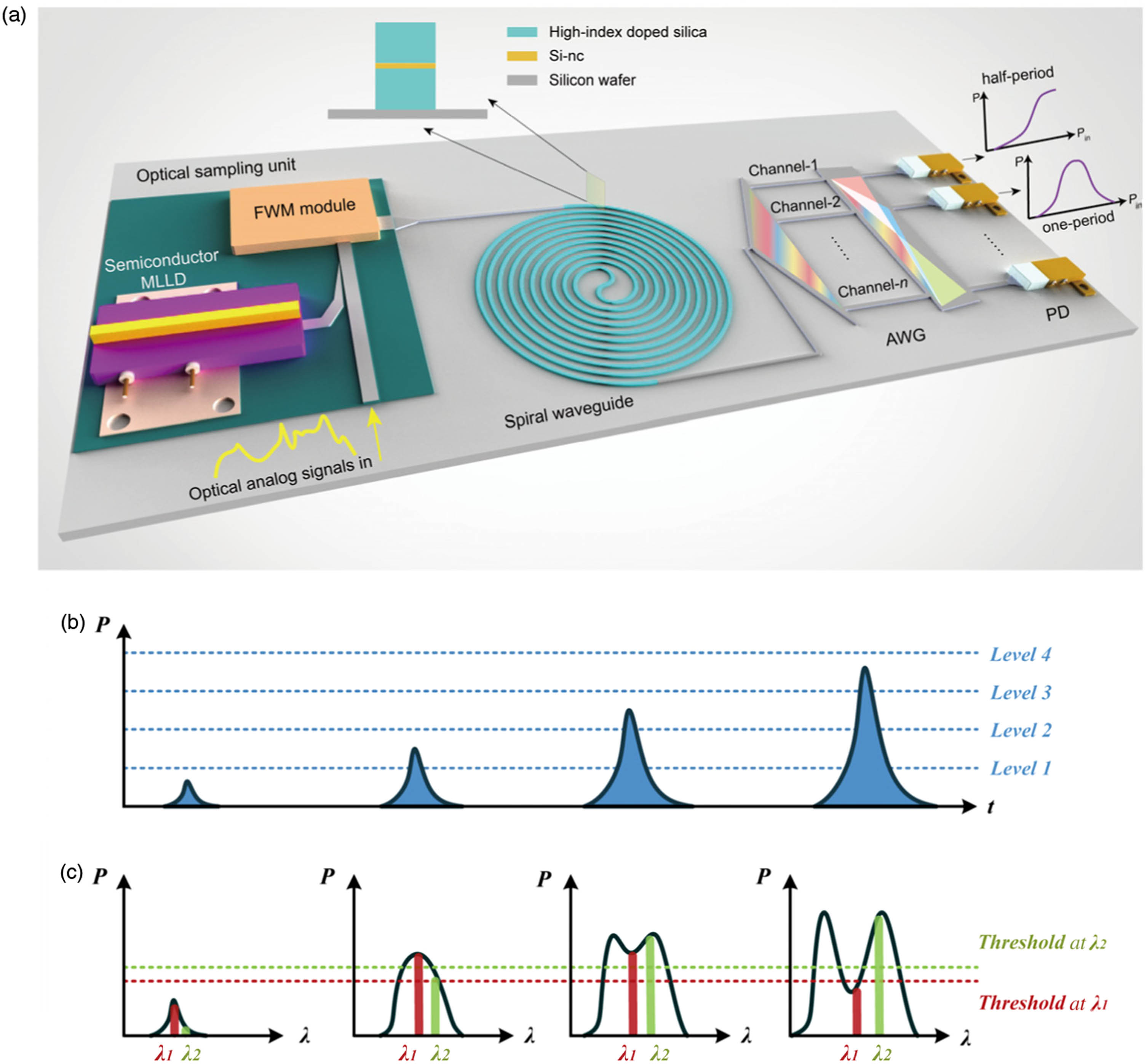
The schematic of the proposed all-optical ADC is shown in Fig. 1. The original analog signal is sampled, using nonlinear sampling processes such as FWM [22,23], into optical pulses at different power levels proportional to the original signal and launched into the proposed quantizer for ADC operation. After propagating through the waveguide, each sampled pulse will experience a power-dependent SPM-induced nonlinear phase shift that leads to different spectral broadening and splitting. By filtering the output spectrum at specific wavelengths with an -channels optical wavelength filter, such as an arrayed waveguide grating (AWG), we can obtain the power transfer functions of the -channels with different periods. Digital codes are generated by combing the binary threshold decision results of the power transfer functions in parallel. Figures 1(b) and 1(c) show an example of a 2-bit ADC. As the power of the sampled pulse is increased, the power transfer function of channel-1 filtered at varies in the way that first increases then decreases to produce a one-period sinusoidal-like variation curve. In contrast, the transfer function of channel-2 filtered at varies only increasingly to produce a half-period sinusoidal-like variation curve. In general, we use only the right-half (or left-half) part of the spectrum for filtering because the broadening and splitting into the two half-parts of the spectrum are quasi-identical. The decision results of channel-1 and channel-2 are assigned to the least significant bit (LSB) and the most significant bit (MSB), respectively. The two decision thresholds of the two quantization channels could be made the same by optimally selecting the filtering wavelengths [24]. We summarize the quantization and coding criterion of a 2-bit ADC in Table 1, where and are the two decision thresholds, is the minimum of the sampled power which is not always zero in practical, and is the power interval of each quantization step.
Sign up for Photonics Research TOC. Get the latest issue of Photonics Research delivered right to you!Sign up now
Figure 1.(a) Schematic diagram of the proposed all-optical ADC. MLLD, mode-locked laser diode; AWG, arrayed waveguide grating; PD, photodiode. (b) Illustrated four sampled pulses with different optical power levels. (c) Corresponding SPM-induced optical spectrum broadening and splitting. Red and green solid lines indicate the filtering wavelengths and of the two quantization channels. Red and green dashed lines indicate the decision thresholds.
The quantization resolution of the proposed ADC depends on the maximum number of the periods of the power transfer function, which is determined by the number of the split dips (or sidelobes) on the half-part of the spectrum. Assuming a total split dips (, 3, 5, …) on the whole spectrum, the ideal number of bit (NOB) is given by . The number “4” indicates the maximum achievable quantization steps in one period of the power transfer function using only binary decision. For example, three split dips are required to obtain an ideal 3-bit NOB. We note that the defined here can be only an odd number since the dip at the center of the spectrum, i.e., the pumping wavelength, is indispensable. Accordingly, should be only an even number if it is defined as the number of the sidelobes. The number of dips induced by the SPM effect only, is approximately given by [27]; here is the SPM-induced maximum phase shift. is the peak power of the pump pulse and is the effective propagation length with the linear loss and the physical length. It is clear that larger nonlinearity, higher power, and lower loss all contribute to larger numbers of dips, which would also increase the NOB. Meanwhile, larger nonlinearity and lower loss also lead to a lower optical power resolution . However, we emphasize that soliton-dominated dynamics in the anomalous dispersion regime can disable the ideal estimation. The ADC has to operate before the soliton fission-induced supercontinuum (SC) generation occurs, which is no doubt a big limitation in practical applications. Therefore, the proposed ADC preferably operates in the normal dispersion regime, which can be realized by tailoring the dispersion of the waveguide through geometrical design. Another significant advantage of operating in the normal dispersion regime is the warranted high coherence of the spectrum, which is crucial in such continuously pumping conditions using many shots sampled-pulses.
3. RESULTS AND DISCUSSION
A. Waveguide Fabrication and Characterization
The proposed quantizer in the ADC with the high-index doped silica glass waveguide with the Si-nc strip was fabricated using a CMOS-compatible high-index glass waveguide fabrication process similar to Refs. [28–30], but with an additional plasma-enhanced chemical vapor deposition amorphous silicon (a-Si) layer deposition step in between two 1 μm thick (measured with the FilmTek™ 4000) high-index doped glass layers. The a-Si film was deposited at 300°C, 349 W, flow rate of 72 sccm at 1 Torr, for 5 s. The multilayer film was then patterned and etched to form the waveguide cores with the designed dimension of 2 μm by 2 μm. The etched core waveguides were then cladded with before they were annealed at 1150°C for 4 h to form the Si-nc in . In the development of the Si-nc fabrication process, samples with different a-Si deposition conditions were annealed right after the deposition of the core layers and without the patterning, etching, and cladding steps. Figure 2(a) shows the transmission electron microscope (TEM) image of the Si-nc film from the optimized Si-nc process with an average grain size of , distributed throughout the film. Lower propagation loss and Si-nc grains with minimum size and uniform distribution for larger nonlinearity can be achieved based on this optimal process [31]. The size of the Si-nc corresponds to an optical bandgap of , or , that results in a negligible nonlinear absorption in the telecom band [32]. Figure 2(c) shows the scanning electron microscope (SEM) image of the waveguide cross section of the fabricated device demonstrating well-formed waveguide structures with an approximately 20 nm thick Si-nc film at the center. The measured waveguide dimensions from the SEM image also show that the annealing process had introduced a 13% shrinkage to the as-deposited waveguides. Using the extracted effective index from the measurement of the 50 GHz microring resonator having the same waveguide geometry as the spiral waveguide and fabricated on the same wafer [33], we estimated the refractive index of the Si-nc layer to be . Figure 2(b) shows the calculated dispersion of the waveguides with and without the Si-nc layer in the center using the measured dimensions. The calculated zero dispersion wavelengths for the quasi-TE polarization are 1175 and 1365 nm for the waveguide without Si-nc, and 1245 and 1340 nm for the case with 20 nm Si-nc, respectively, where both waveguides show a wide span of normal dispersion at the telecom regime that is advantageous for the proposed ADC operation. Figure 2(d) shows that the simulated quasi-TE polarization mode profiles have the fields tightly confined inside the high-index doped silica glass layers and the Si-nc layer.
Figure 2.(a) TEM image of the Si-nc film before depositing the upper layer of high-index doped silica glass. Inset: an individual silicon nanocrystal of in dimension. (b) Calculated dispersion for the waveguides for the quasi-TE polarization. (c) SEM image for the waveguide with a thin layer of 20 nm Si-nc in the core center. (d) Corresponding simulated electric field profile of the quasi-TE polarization.
Since the principle of the proposed waveguide structure with the Si-nc strip is in the optimization between the enhanced nonlinear effect due to the Si-nc layer and the associated linear and nonlinear losses it incurs, both linear and nonlinear characterizations of the fabricated waveguide devices were carried out to investigate this trade-off. In the linear loss characterization, the half-slope of the reflectivity data of the coherent optical frequency domain reflectrometry (OFDR) measurement (Luna, OVA 5000 & OFDR) with respect to propagation length [34] is used to determine the propagation loss of the fabricated waveguides, as shown in Fig. 3(a). The spiral waveguide has a minimum bending radius of 200 μm and 8 μm gap between the adjacent circles. This approach allows us to reduce the measurement uncertainty associated with the variation of the fiber-to-waveguide coupling in the conventional cutback measurement method. Table 2 shows the comparison of the propagation loss between the waveguides with and without the Si-nc layer, where the measured propagation loss of the waveguide with the Si-nc strip is 0.16 dB/cm for the TE modes. As compared to the conventional uniform waveguide, the introduction of the thick layer Si-nc film adds an additional 0.06 dB/cm propagation loss in the 1550 nm range. From the extracted fiber-to-waveguide coupling loss values, the Si-nc film also adds an average of 0.7 dB/facet coupling loss due to the tighter mode confinement. The added fiber-to-waveguide loss is not a major concern as it can be reduced with a proper designed mode transformer once the optimized waveguide geometry is identified. It should be noted that the waveguide with the Si-nc strip only operates in the TE mode as the TM mode suffers much higher propagation loss () due to the scattering from the Si-nc layer.
Figure 3.(a) OFDR trace from the long spiral waveguide pigtailed to the fiber array. The in/through ports of the spiral waveguides can be clearly identified as the high peaks at the beginning and end of the recorded traces. The linear fit of the waveguide backscattering (the short-dotted line) is performed over a wavelength range of 1525–1567 nm, the half-slope of which gives the propagation loss. Moreover, the linear relationship reflects the neglectable bending loss. The extent of loss fluctuation of the waveguide with the Si-nc strip is almost the same as that without the strip case, indicating high quality of the nanocrystal layer in the core center. (b) Reciprocal transmission as a function of the coupled peak power. Solid lines represent the fitting results. (c) FWM spectrum recorded by OSA for the spiral waveguide without Si-nc. (d) Conversion efficiency as a function of pump power. Dots: experimental results; solid lines: linear fitting results.
In the nonlinear characterization, the nonlinear absorption due to two-photon absorption (TPA) is measured using a shape pulsed laser and by the fitting of the reciprocal transmission peak [35] to obtain the TPA coefficient , with where is the linear loss, is the nonlinear coefficient, and is the effective area of the spiral waveguide. Figure 3(b) shows the experimental results from the 51.66 cm long spiral waveguide. The measured are and for the waveguides with and without the 20 nm Si-nc layer, respectively. Although there is a fivefold increase of the with the Si-nc layer compared to the conventional waveguide, TPA is still negligible in the waveguides with the Si-nc strip as the measured is more than 5 orders of magnitude lower than that of the hydrogenated amorphous silicon, which already shows negligible nonlinear absorption [36].
To quantify the amount of nonlinear enhancement with the addition of the Si-nc layer in the waveguide, the FWM method is used to determine the real part of the nonlinear coefficient [37], where the conversion efficiency is related to by where is the propagation length and , , and represent the propagation constants of the pump, the signal, and the idler, respectively. Figures 3(c) and 3(d) show the measured FWM spectrum and conversion efficiency as a function of pump power for the fixed pump and signal wavelengths. The result in Fig. 3(d) shows increased by in the waveguide with the Si-nc strip, which corresponds to an approximately threefold increase in the nonlinear coefficient with the introduction of a thin 20 nm Si-nc layer in the waveguide core, shown in Table 2.
Different from the conventional horizontal slot waveguide structures that localize the field in the slot and waveguide interface to enhance the nonlinearity [24,38,39], the proposed waveguide focuses on an optimized approach by increasing the nonlinearity through the localized field while limiting the scattering loss from the surface interfaces at the same time. Although the difference of refractive index between the high-index doped silica glass layers and the Si-nc layer is , the thickness of the strip layer is only ; thus, a large fraction of light can leak into the high-index doped silica glass layers to acquire a low loss. Meanwhile, we can still achieve significant nonlinearity enhancement with a small trade-off in propagation loss.
B. All-Optical ADC Analysis
Figure 4(a) shows the experimental setup of the demonstration for the quantization of the all-optical ADC. Instead of the schematic shown in Fig. 1 with separate mode-locked laser diode, FWM module, and an external optical signal input, a femtosecond fiber laser (FFL, PriTel) is used with a variable optical attenuator (VOA) to recreate a sampled optical signal. In the experiment, the pump pulse emitted from the FFL has a pulse width of 390 fs and a repetition rate of 20 MHz. The VOA is followed to adjust the peak power of the pulses. We note that the current experiment is not a “real-time” ADC operation. A polarization controller is used to guarantee TE polarization state of the light injected into the spiral waveguide. We do not use an erbium-doped fiber amplifier (EDFA) to create a scenario of real on-chip integration since there is still no promising on-chip amplifiers for Group IV materials-based waveguides. Another reason is that the evolved complex spectrum after the EDFA is not conducive to the proposed ADC. The pump wavelength is also arbitrarily set to 1558 nm to show the performance of the ADC. In fact, the proposed ADC scheme can work well without specific wavelength limitation, as long as the pump wavelength is located in the normal dispersion regime, as shown in Fig. 2(b). Figure 4(b) shows the measured spectra when three pulses with different peak power levels, i.e., 1.1, 45.9, and 95.7 W, respectively, are injected into the 50 cm Si-nc loaded waveguide. The gray dashed curve in Fig. 4(b) shows the initial spectrum of the input pump pulse with 95.7 W peak power. We observe that the output spectrum is first broadened, and then split out into two sidelobes (or one dip in the middle) when the input peak power is increased from 1.1 to 95.7 W. The degree of the broadening and splitting of the spectrum is proportional to the power levels of the input pulses, thus mapping the temporal power variation to the spectral variation. Two sidelobes (one dip) correspond to 2-bit NOB as discussed in the principle. A 50:50 coupler is used to connect the through port of the spiral waveguide to the two receivers for the MSB and LSB. We filter the spectrum output from the waveguide by using two optical filters of 0.65 nm passband (Santec, OTF-30M-08S2) that are centered at 1557 and 1558 nm, respectively. The filtered light is assigned to the two quantization channels and detected by the photodiodes to create the two parallel binary codes. It should be noted the central wavelengths of the filters need to be tuned according to the pump wavelength, since the two quantization channels locate around. Figure 4(c) shows the power transfer functions of the two quantization channels measured in the experiment. For the input peak power range from 10 to 94 W, the approximate one- and half-period power curves are obtained. We find the same decision threshold of 0.36 can be used to simultaneously achieve the binary codes of the two quantization channels. Figures 4(d) and 4(e) show the power transfer function together with the binary decision results of the two channels, respectively. For channel-1 shown in Fig. 4(d), the input peak power ranges 10–31 W and 73–94 W are finally encoded to “0,” while the power range 31–73 W is encoded to “1.” In parallel, Fig. 4(e) shows the input peak power of channel-2 range 10–52 W is encoded to “0,” while the power range 52–94 W is encoded to “1.” Final Gray codes of 00, 01, 10, and 11 are obtained by combining the codes of the two channels. We find the power interval of the four quantization steps is perfectly uniform. By using the method in Refs. [3,24], the effective number of bits (ENOB) is estimated to be 1.998-bit. With the proposed nonlinearity-enhanced waveguide, the highest average power to achieve the demonstrated 2-bit quantizer is only 0.72 mW, with a peak power of 94.2 W and energy consumption of 19.55 pJ/bit. For the complete ADC system, one needs to include the 6 dB loss of the external coupler and coupling loss into the waveguide resulting in the total power consumption of 2.87 mW average power, 375.3 W peak power, and energy consumption of 77.91 pJ/bit.
Figure 4.(a) Experimental setup (FFL, femtosecond fiber laser; VOA, variable optical attenuator; PM, power meter). (b) Measured spectral profiles at the output of the 50 cm Si-nc loaded waveguide (μμ) with different input pump peak powers. (c) Measured power transfer functions of the two quantization channels by filtering the spectrum at the wavelengths of 1557 and 1558 nm, respectively. (d),(e) Power transfer functions of the two channels with binary decision results.
In order to see more detailed dynamics and features that are difficult to obtain in our experiments due to the limitation of the existing experimental devices, we simulate the spectrum splitting process in the proposed waveguide with the Si-nc strip using the nonlinear Schrödinger equation [24]. The nonlinear absorption is safely neglected as characterized in the above experiments. The simulation parameters are the same as those shown in Fig. 4 except the wavelength-dependent dispersion and nonlinear coefficients. Three pumping wavelengths of 1550, 1558, and 1565 nm in the normal dispersion region are arbitrarily chosen for illustration. The group velocity dispersion parameters are calculated to be , 70.5, and , respectively, at 1550, 1558, and 1565 nm. The corresponding nonlinear coefficients are , 305, and , respectively. The third- and fourth-order dispersion parameters of all three wavelengths are calculated to be and , respectively. The peak power of the hyperbolic secant pump pulse is fixed to 95.7 W. Figure 5(a) shows the simulated spectral profiles at the output end of the waveguide when pumping at 1550, 1558, and 1565 nm, respectively. As compared to the experimental results pumped at 1558 nm, we find that the simulation results coincide to the experimental ones. The differences on the envelope of the spectrum are attributed to the nonideal hyperbolic secant profile of the initial pump pulse in the experiments. We find that the spectra obtained at the three pumping wavelengths show less difference, which confirms the flexibility of the scheme on pumping wavelength selection. The advantage benefits from the flattened dispersion and nonlinear characteristic of the proposed waveguide within this telecom band. Figure 5(b) shows the corresponding temporal profiles at the three pumping conditions. In contrast to the distinct splitting of the spectra, the temporal profiles only evolve to smooth Gaussian-like shapes without any energy leaking or pulse breaking. It benefits from pumping in the normal dispersion regime, where the soliton-induced complex dynamics are avoided.
Figure 5.Simulated (a) spectral and (b) temporal profiles when pumping at 1550, 1558, and 1565 nm, respectively. The wavelength axis of the spectral profiles is normalized to the pumping wavelengths.
Figures 6(a)–6(d) show the simulated spectrograms at pump peak powers of 35, 95.7, 220, and 380 W, respectively, to simultaneously see the temporal and spectral performances. When the pump peak power is increased, the spectra keep broadening and splitting out more dips on the tops. Figures 6(c) and 6(d) show that two and three dips (at half-part of the spectrum) are obtained at the peak powers of 220 and 380 W, respectively, which indicates achievable two and three periods of the power transfer function and correspondingly ideal NOB more than 3-bit. Larger NOBs are predictable as long as more dips are split out before evolving into complex SC process. We have included the stimulated Raman scattering effect in our simulation, but do not observe any obvious influence on spectral broadening and splitting even at the peak power as high as 2000 W, in which case 23 dips are generated in the whole optical spectrum corresponding to an ideal NOB of 5.59-bit. We believe the proposed waveguide confines most of the optical power in the middle Si-nc layer, which inherently has weak Raman response similar to silicon [40]. Even for the cases that Raman effect does occur, we can still use TM modes instead, in which the Raman scattering is absent [41]. We note that in our experiments we failed to obtain ideal spectrum splitting results with two dips or more. It is because the on-chip pump peak power without assistance of EDFA is limited to 95.7 W. More dips require larger peak power to produce enough nonlinear phase shift. However, the pump pulse acquires nonlinear evolution during the amplification in the EDFA, which leads to complex temporal and spectral profiles rather than the ideal hyperbolic secant shape. Consequently, the spectrum broadening and splitting processes also become more complex. We also note that the outboard spectral sidelobes have wider linewidths, i.e., the oscillation period of the split spectral sidelobes is not a constant. As a result, the period of the power transfer function might not be a constant when the pump peak power is increased, which will degrade the ENOB. In the time domain, the pulse profiles change only a little for the peak power of several tens of watts. For the higher peak power up to hundreds of watts, the tops of the pulse profiles gradually change shape to flattened structures. However, we emphasize that there are still no redundant sidebands or complex structures arising. The energy of the pulse is highly concentrated in the central region. Such a characteristic contributes to the advantage that the power difference among the different quantization channels filtered out from the spectrum can be very small. Thus, binary decision of all the quantization channels using an identical threshold becomes more feasible.
Figure 6.Simulated spectrograms at the pump peak power of (a) 35 W, (b) 95.7 W, (c) 220 W, and (d) 380 W, respectively. di, , 2, 3, indicates the number of dips on the half-part of the spectrum.
In summary, we propose a CMOS-compatible all-optical ADC based on a high-index doped silica glass waveguide with a Si-nc strip. The linear and nonlinear characteristics of the waveguide are investigated experimentally, which shows the advantages of low loss, large nonlinearity, and negligible nonlinear absorption. Experimental results successfully demonstrate the proposed ADC with 2-bit resolution at the low pump peak power of 95.7 W. Simulation results are further shown to confirm the flexibility of the proposed ADC in a broad spectrum band and the achievable larger NOB. Even with only the 2-bit ADC basic unit, the resolution can be efficiently increased by employing the cascade optical quantization operation [42]. We emphasize that each individual component in this all-optical ADC could be fabricated using high-index doped silica glass or Group IV materials-based CMOS-compatible platforms. For example, the filter array for spectrum extraction can be realized by a microring array or AWG, and the TE polarizer can be realized by vertical slot waveguides. The same is true to the variable attenuator and the coupler. It means the whole ADC has great potential to be monolithically integrated on a single chip, which is unattainable to fiber-based ADCs. The excellent characteristics of the proposed waveguide make it not only a promising all-optical ADC but also serve as other power-efficient nonlinear functional devices in advanced information systems.
Yuhua Li, Kun Zhu, Zhe Kang, Wai Lok Ho, Roy Davidson, Chao Lu, Brent E. Little, Sai Tak Chu, "CMOS-compatible high-index doped silica waveguide with an embedded silicon-nanocrystal strip for all-optical analog-to-digital conversion," Photonics Res. 7, 1200 (2019)