Abstract
In this paper, we study an original strategy to generate an infrared waveband microlaser by an integrated III–V-nanowire (NW)-based photonic array for on-chip interconnects. The optical modes of the III–V-NW-based photonic array are investigated for utilization as an all-in-one gain medium, waveguide, and cavity. Adequate designs of periodic arrays of InP NWs with different polarization TM and TE modes are studied by 3D electromagnetic simulation finite difference time domain to optimize the resonant active photonic crystal (hybrid Bloch modes) in the infrared band at 1.3 μm. According to our calculations, NWs larger than 0.2 μm in diameter are needed to conceive optic modes inside NW photonics in TM polarization. However, smaller NW photonics, such as 0.1 μm in diameter, can obtain only the TE mode inside the NWs. This phenomenon is theoretically illustrated by the dispersive curves of NW-based photonics. It aims at demonstrating that the slow velocity mode inside the NW photonics will cause amplification of lightwaves and generate microlasers in the infrared band at 1.3 μm. These studies are of prime importance for further microlaser integration to silicon-on-insulator (SOI) waveguides for on-chip optical interconnects.1. INTRODUCTION
Silicon is the main material used in semiconductor manufacturing today and CMOS technology will probably go on dominating the electronic market for many decades. However, with the size reduction of transistors, one of the most critical issues is related to metallic contacts and interconnects. The thermal budget in the multilayered metallic links above Si transistors hinders their further miniaturization. A technological breakthrough is necessary. The integration of optical links with active photonic material on the Si wafer for high-speed optical interchip and intrachip connects is a possible route to economic the CMOS industry for low-power consumption with next-generation communication technologies.
Semiconductor nanowires (NWs) are considered to be the next frontier for ultrasmall, highly efficient coherent light source lasers to reduce the footprint of devices for 3D device integration and hence are being extensively studied in the context of optoelectronic devices [1–3] and nanophotonic circuits [2,4], such as waveguides, LEDs, nanolasers, and optical switches [5–18]. Recently, single semiconductor NW lasers have been realized in various materials, with emission wavelengths ranging from the ultraviolet to infrared for their widely available bandgaps [1–3]. Stationary photoluminescence (PL) studies conducted by Reitzenstein et al. [19] as well as time-resolved PL studies [20] have shown good optical properties for InP NWs grown on Si (001) by metal-organic vapor-phase epitaxy, which is a good prerequisite for the realization of an optical emitter. However, NW-array-based photonic lasers have been rarely studied. Cylindrical active III–V NWs with a diameter of several hundreds of nanometers and a length of micrometers can efficiently confine and guide optic waves inside the gain medium on a nanometer scale, and they can also allow the integration of optically active III–V semiconductors onto existing silicon technologies despite a large mismatch in the lattice constant. The photonic NW array structure, on the other hand, can form a microsource cavity to get slow group velocity mode for high optical energy generation inside a gain medium. All of these properties induce the possible realization of nanophotonic lasers as coherent light microsources for integrated on-chip photonics.
Our work proposes an original strategy to generate an infrared waveband microlaser by integrated III–V-NW-based photonic arrays for on-chip interconnects. The optical properties of NW-based photonic arrays are optimized for utilization as an all-in-one gain medium, waveguide, and cavity. Adequate designs of periodic arrays of InP NWs with different polarization TM and TE modes were studied by 3D electromagnetic simulation finite-difference time-domain (FDTD). The geometrical parameters of this architecture are optimized to obtain modes in the infrared band. A regular array of such NWs will form a resonant active photonic crystal (hybrid Bloch modes). Our work aims at demonstrating that, under optical pumping, the slow velocity mode inside the NW photonics will cause amplification of lightwaves and generate a microlaser in the infrared band at 1.3 μm. This ultracompact source of the original architecture is expected to have an enhanced global efficiency and reduced power consumption, which is of prime importance in the field of silicon photonics.
Sign up for Photonics Research TOC. Get the latest issue of Photonics Research delivered right to you!Sign up now
2. NW PHOTONIC ARRAY DEFINITION AND OPTICAL POLARIZATIONS
The infinite periodic NW array was studied separately with TM and TE polarizations by 3D FDTD simulation. In our calculations, the wave propagation is set in the direction. So, for the TM mode, the main electronic field is in the direction (see Fig. 1) and and are in the plane, which is vertical to the axis. In TE mode, the electronic field is set in the plane ( and ), and is the main part of the electronic field in the propagation. In other words, for TM mode, the main electronic field is perpendicular to these NWs; for TE mode, the main electronic field is parallel to these NWs. According to the periodic photonic structure, the periodic boundary condition is used to optimize the calculations. The slow group velocity modes and their field distributions inside the NW chain system were studied with various dimensions of NW diameter and different source polarization TM and TE modes.
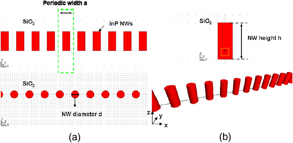
Figure 1.(a) Photonics array with an infinite number of InP NWs and (b) InP NWs () in a environment ().
3. DISCUSSION
In both TM and TE polarizations, the fundamental mode wavelength of the NW photonic array increased with the photonic periodic length . There is stronger redshift with TE than with TM polarization when the NW diameter is increased. For NWs with diameter , photonic periodic length needs to be chosen as 0.4 μm for TM and 0.33 μm for TE in order to achieve a 1.3 μm resonance mode for our laser. From the electric energy distribution in the NW profile and its cross section, an apparently optical mode can be observed inside the NWs. The E energy is strongly restrained inside the NWs. Furthermore, for smaller NWs, should be wider, up to 0.42 μm for both TM and TE polarizations to obtain modes in the resonance region that are widely used in optic telecommunication. It is very interesting that in the NW photonic array, strong TE modes exist inside the NWs with diameters of both 0.2 and 0.1 μm; however, TM mode with 0.1 μm NWs is very weak, as shown in Fig. 2(a).

Figure 2.Optical modes in a NW photonics array with various NW diameters and photonic periodic lengths in (a) TM and (b) TE polarization.
Figure 3 shows the spectra of the TM mode with NW diameters varying from 0.1 to 0.2 μm. The resonance of each mode of the NW photonic array redshifts with increased NW diameter . The larger the NWs, the stronger is the E energy intensity inside each mode. That is exactly what we observed in Fig. 2(a).
Figure 3.TM mode spectrum and its mode with different NW diameters .
A. Wave Vector β Effect
To explore guided modes in the NWs at the edge of ZB to get a slow group velocity mode for high energy, wave vector is studied from 0.9 to 1 (see Table 1). Here, is fixed to 0.4 μm.
| d=0.1 μm | β (π/a) | 0.9 | 0.92 | 0.95 | 0.97 | 0.98 | 0.99 | 1 |
| Lambda (μm) | 1.3561 | 1.3299 | 1.2897 | 1.2626 | 1.2488 | 1.2367 | 1.2263 |
| d=0.2 μm | β (π/a) | 0.9 | 0.92 | 0.95 | 0.97 | 0.98 | 0.99 | 1 |
| Lambda (μm) | 1.3752 | 1.3545 | 1.3215 | 1.3028 | 1.2962 | 1.2929 | 1.2913 |
Table 1. TM Mode Resonance Wavelengths with Different Wave Vectors
1. TM Mode
From the dispersion curve in Fig. 4, we can see that the group velocity changes a lot with the NW diameter. The slow group velocity mode with high energy exists in , however, in the case, no slow group velocity mode exists. Compared to the only space (green line), the modes in the NW photonic array with are almost the same as that in space, which both reach when . This indicates that the slow group velocity mode cannot exist inside NWs with in TM mode. As the TM mode band is so close to the light line, there are extended states in both the dielectric environment and the NWs. The optic energy passes through the whole structure and no mode exists inside the NWs array.
Figure 4.TM modes with different wave vectors .
Figure 5.TE modes with different wave vectors .
This situation is different in TE mode.
2. TE Mode
In TE mode, periodic length is fixed to 0.33 μm (see Table 2). In this mode, different NW diameters will change the mode energy inside. However, the slow group velocity modes exist in both the and cases. That is why a strong field and energy mode can be found in TE mode with both and , whereas in TM mode, the mode exists only in the NW system with (see Fig. 5).
| d=0.1 μm | β (π/a) | 0.9 | 0.92 | 0.95 | 0.97 | 0.98 | 0.99 | 1 |
| Lambda (μm) | 1.1371 | 1.1179 | 1.0928 | 1.0813 | 1.0779 | 1.0756 | 1.0750 |
| d=0.2 μm | β (π/a) | 0.9 | 0.92 | 0.95 | 0.97 | 0.98 | 0.99 | 1 |
| Lambda (μm) | 1.3342 | 1.3230 | 1.3103 | 1.3045 | 1.3028 | 1.3011 | 1.3003 |
Table 2. TE Mode Resonance Wavelengths with Different Wave Vectors
4. CONCLUSION
The optical modes of a III–V-NW-based photonic array are studied for utilization as an all-in-one gain medium, waveguide, and cavity. The geometrical parameters of this architecture are optimized to obtain modes in the infrared band at 1.3 μm. The regular array of such NWs formed a resonant active photonic crystal (hybrid Bloch modes). According to our 3D electromagnetic FDTD calculations, bigger NWs, such as 0.2 μm in diameter, are needed to conceive optic modes inside NW photonics in TM polarization. However, smaller NW photonics, such as 0.1 μm in diameter, can also be used in TE mode to obtain strong optic energy inside the NWs. This phenomenon is theoretically illustrated by the dispersive curves of NW-based photonics. These studies are of prime importance for further microlaser integration to silicon-on-insulator waveguides for on-chip optical interconnects.
ACKNOWLEDGMENT
Acknowledgment. This work is funded by the French Research National Agency (ANR) through the INSCOOP project (ANR-11-NANO-012).
References
[1] D. Saxena, S. Mokkapati, P. Parkinson, N. Jiang, Q. Gao, H. H. Tan, C. Jagadish. Optically pumped room-temperature GaAs nanowire lasers. Nat. Photonics, 7, 963-968(2013).
[2] R. Yan, D. Gargas, P. Yang. Nanowire photonics. Nat. Photonics, 3, 569-576(2009).
[3] P. Yang, R. Yan, M. Fardy. Semiconductor nanowire: what’s next?. Nano Lett., 10, 1529-1536(2010).
[4] P. J. Pauzauskie, P. Yang. Nanowire photonics. Mater. Today, 9, 36-45(2006).
[5] M. Law, D. J. Sirbuly, J. C. Johnson, J. Goldberger, R. J. Saykally, P. Yang. Nanoribbon waveguides for subwavelength photonics integration. Science, 305, 1269-1273(2004).
[6] J. Bao, M. A. Zimmler, F. Capasso, X. Wang, Z. F. Ren. Broadband ZnO single-nanowire light-emitting diode. Nano Lett., 6, 1719-1722(2006).
[7] M. H. Huang, S. Mao, H. Feick, H. Yan, Y. Wu, H. Kind, E. Weber, R. Russo, P. Yang. Room-temperature ultraviolet nanowire nanolasers. Science, 292, 1897-1899(2001).
[8] C. Z. Ning. Semiconductor nanolasers. Phys. Status Solidi B, 247, 774-788(2010).
[9] M. A. Zimmler, F. Capasso, S. Muller, C. Ronning. Optically pumped nanowire lasers: invited review. Semicond. Sci. Technol., 25, 024001(2010).
[10] J. C. Johnson, H.-J. Choi, K. P. Knutsen, R. D. Schaller, P. Yang, R. J. Saykally. Single gallium nitride nanowire lasers. Nat. Mater., 1, 106-110(2002).
[11] X. Duan, Y. Huang, R. Agarwal, C. M. Lieber. Single-nanowire electrically driven lasers. Nature, 421, 241-245(2003).
[12] A. H. Chin, S. Vaddiraju, A. V. Maslov, C. Z. Ning, M. K. Sunkara, M. Meyyappan. Near-infrared semiconductor subwavelength-wire lasers. Appl. Phys. Lett., 88, 163115(2006).
[13] Y. Xiao, C. Meng, P. Wang, Y. Ye, H. Yu, S. Wang, F. Gu, L. Dai, L. Tong. Single-nanowire single-mode laser. Nano Lett., 11, 1122-1126(2011).
[14] B. Piccione, C.-H. Cho, L. K. van Vugt, R. Agarwal. All-optical active switching in individual semiconductor nanowires. Nat. Nanotechnol., 7, 640-645(2012).
[15] R. F. Oulton, V. J. Sorger, T. Zentgraf, R.-M. Ma, C. Gladden, L. Dai, G. Bartal, X. Zhang. Plasmon lasers at deep subwavelength scale. Nature, 461, 629-632(2009).
[16] Y.-J. Lu, J. Kim, H.-Y. Chen, C. Wu, N. Dabidian, C. E. Sanders, C.-Y. Wang, M.-Y. Lu, B.-H. Li, X. Qiu, W- H. Chang, L.-J. Chen, G. Shvets, C.-K. Shih, S. Gwo. Plasmonic nanolaser using epitaxially grown silver film. Science, 337, 450-453(2012).
[17] G. Wang, X. Jiang, M. Zhao, Y. Ma, H. Fan, Q. Yang, L. Tong, M. Xiao. Microlaser based on a hybrid structure of a semiconductor nanowire and a silica microdisk cavity. Opt. Express, 20, 29472-29478(2012).
[18] B. Mayer, D. Rudolph, J. Schnell, S. Morkötter, J. Winnerl, J. Treu, K. Müller, G. Bracher, G. Abstreiter, G. Koblmuller, J. J. Finley. Lasing from individual GaAs-AlGaAs core-shell nanowires up to room temperature. Nat. Commun., 4, 2931-2938(2013).
[19] S. Reitzenstein, S. Münch, C. Hofmann, A. Forche, S. Crankshaw, L. C. Chuang, M. Moewe, C. Chang-Hasnain. Time resolved microphotoluminescence studies of single InP nanowires grown by low pressure metal organic chemical vapor deposition. Appl. Phys. Lett., 91, 091103(2007).
[20] S. Crankshaw, S. Reitzenstein, L. C. Chuang, M. Moewe, S. Münch, C. Böckler, A. Forchel, C. Chang-Hasnain. Recombination dynamics in wurtzite InP nanowires. Phys. Rev. B, 77, 235409(2008).


