
Jian Fan, Xuyan Zhou, Weiqiao Zhang, Yufei Wang, Hongwei Qu, Aiyi Qi, Wanhua Zheng, "Improving the performance of high-power broad-area lasers by suppressing cavity modes propagating in the lateral dimension," Chin. Opt. Lett. 21, 041406 (2023)
- Chinese Optics Letters
- Vol. 21, Issue 4, 041406 (2023)
Abstract
1. Introduction
Currently, semiconductor diode lasers are the laser light source with the highest electro-optical conversion efficiency and with advantages of high power, long lifetime, small size, low cost, and easy integration[1–3]. Semiconductor diode lasers have been widely used in many fields, such as optical communications, optical pumping, optical storage, laser printing, and laser cutting[4–6]. The typical commercial structure of high-power semiconductor diode lasers is the broad-area (BA) lasers. The current wall-plug efficiency (WPE) of a high-power BA laser can reach more than 75%[7]. We refer to a BA single emitter with a large gain stripe width as a superlarge mode field (SLMF) laser. SLMF lasers have many advantages. With high power and low horizontal far-field divergence, SLMF lasers can be used directly as a laser source and pumping source for fiber with high coupling efficiency. SLMF lasers have better beam quality than laser bars, which can reduce the complexity of beam combining adapted to most beam-combining systems. However, SLMF laser devices easily suffer from abnormal threshold currents, failure to lase, abrupt deterioration, and rapid thermal saturation. Because the physical environment of the BA laser is complex, it is affected by the following factors: thermal lensing[8,9], spatial hole burning[10], and filamentation[11,12]. We previously reported the realization of a low-coherence laser by tuning the non-Fabry–Perot mode of the resonant cavity[13].
In our work, we designed a sidewall sawtooth cavity (SSC) structure: a one-dimensional triangular array on both sides of the gain stripe to suppress the lateral resonant mode. This structure was previously used to improve beam quality by suppressing higher-order lateral modes[14]. However, we use this structure to suppress the cavity modes propagating in the lateral dimension. To the best of our knowledge, this approach is the first that has been proposed to study high-power semiconductor lasers. In the theoretical simulation, we used wave-dynamical chaos theory[11,13] to calculate resonant optical modes of the SSC cavity and the standard Fabry–Perot (F–P) cavity. We analyze the mode difference and characterize the scattering loss of the lateral resonant mode using the Q factor. We demonstrate that the sawtooth microstructure can effectively prevent the optical feedback of the lateral resonant modes. Experimentally, a conventional BA laser and an SSC laser are fabricated. Compared with conventional BA lasers, SSC lasers have a 15% lower threshold current, 0.04 W/A higher slope efficiency, and 23% higher output power at 8 A under continuous current. The amplified spontaneous emission (ASE) spectrum of SSC lasers is narrowed by 50% compared to conventional BA laser. At 48 A, the maximum output power of the SSC laser is 43.03 W, which is about 1 W higher than the standard BA laser.
2. Design and Fabrication
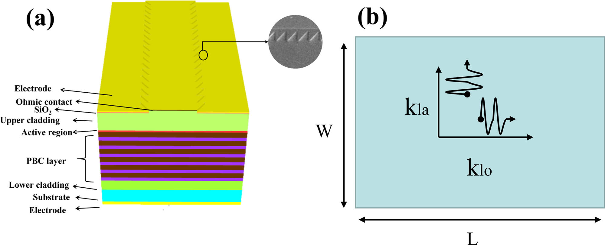
The schematic diagram of the three-dimensional structure of the device is shown in Fig. 1. In the epitaxial direction, we add a photonic band crystal (PBC) structure[15,16] in the N-type region, and the wafer is grown by metal organic chemical vapor deposition (MOCVD) on a GaAs substrate. The active layer contains two
Sign up for Chinese Optics Letters TOC. Get the latest issue of Chinese Optics Letters delivered right to you!Sign up now
![]()
Figure 1.(a) Schematic diagram of SSC laser. The inset is the scanning electron microscope (SEM) image of the fabricated SSC structure. (b) Sketch of a rectangular F–P cavity of length L and width W. The wave vector can be separated into longitudinal and lateral components klo and kla, respectively.
In terms of simulation, we use commercial COMSOL software to calculate the lateral resonant mode of the standard F–P cavity and the SSC cavity. We calculate a two-dimensional cavity. The perfect electric conductor boundary condition is used. The refractive index of the active region is 3.564, which is the effective refractive index of the fundamental mode. The material of the passive region is set to air and the refractive index is 1. The width of the entire simulation area is 42 µm and the length is 52 µm. In an F–P cavity, the wave vector can be separated into longitudinal and transverse components
![]()
Figure 2.The typical lateral oscillation mode distribution in the F–P cavity and the SSC cavity. The width is 40 µm, and the length is 50 µm; both the width and length of the triangle are 2 µm.
![]()
Figure 3.Calculated Q-factors of the lateral propagating modes in the SSC cavity (black dots) and the F–P cavity (red dots).
The calculated Q-factors of the lateral propagating modes in the SSC cavity (black dots) and the F–P cavity (red dots) are shown in Fig. 3, respectively. The Q-factors of longitudinal propagating modes with the order number of
3. Device Characteristic and Discussion
We fabricate SSC lasers and BA lasers on the same wafer. Both SSC and BA lasers have a stripe width of 300 µm. The cavity length is 4 mm, and the cavity facet is not coated. Since the sawtooth microstructure of the SSC laser and the gain area are done by one-step inductively coupled plasma (ICP) etching, the SSC structure and the gain area coincide. These devices are mounted P-side down with AuSn solder on aluminum nitride heat sinks. Figure 4(a) displays the L-I-V characteristic curves of the four types of lasers measured at the room temperature under the continuous-wave (CW) operation. The sizes of the three structures of the SSC laser are shown in Fig. 4(b). The performance of the SSC laser is significantly better than that of the standard BA laser. The device with structure 2 (cyan solid line) has the best performance among the devices with triangle microstructures. Consequently, we compared the SSC laser with structure 2 with the standard BA laser (orange solid line). The threshold current of the standard BA laser is 2.18 A. The devices with structure 2 have the lowest threshold current, which can be as low as 1.83 A. Compared with the threshold current of the standard BA laser, the threshold current of the SSC laser is reduced by nearly 15%. The output power of the SSC laser is up to 2.26 W at injection current of 8 A, which is about 23% higher than that (1.83 W) of the standard BA laser. The slope efficiency of the chosen SSC laser is about 0.40 W/A, but that of the standard BA laser is only 0.36 W/A. The voltage curves of the SSC laser and the standard BA laser are almost the same because the injection window area of devices is the same. The devices used in the next experiments are the SSC laser with structure 2.
![]()
Figure 4.(a) L-I-V characteristic curves of the four types of lasers measured at room temperature under the CW operation; (b) three microstructures with different sizes.
To more clearly characterize the reduction of the lateral propagating modes, we fabricate a special device, similar to a superluminescent diode[18]. The two cleaved faces of devices are coated with an antireflection layer, the transmittance of which is 97%. The ASE spectrum of devices is measured, as shown in Fig. 5. In the ASE spectrum, there is not much variability in the competition between modes, which can be observed visually. It can be seen from Fig. 5(a) that the ASE spectrum of the standard BA laser shows asymmetry on both sides of the lasing peak. This may be caused by the modal gain spectrum of the device[19–21]. The gain space at the short wavelength (the left of the lasing peak) is larger than that at the long wavelength (the right of the lasing peak).
![]()
Figure 5.The ASE spectrum of the SSC lasers and the standard BA lasers at (a) 1.5 A and (b) 2.3 A, respectively.
Therefore, the asymmetric gain spectrum causes the uneven energy distribution on both sides of the lasing peak in the ASE spectrum. The SSC laser has improved the unequal effect of energy distribution, and the energy assigned to the frequency on both sides of the lasing peak is reduced, namely, more available gain is obtained by the main oscillation mode. When the measured current increases from 1.5 to 2.3 A, we find that the FWHM of the ASE spectrum of the SSC lasers is much smaller than that of the ASE spectrum of the standard BA lasers. Figures 5(a) and 5(b) show that the FWHM of the ASE spectrum of the SSC lasers is nearly 50% narrower than that of the SSC lasers. As the test current increases, the FWHM of the BA laser decreases from 26.2 to 17.5 nm, while the FWHM of the SSC laser remains between 13.2 and 9.68 nm. The above results indicate a reduction in the number of SCC cavity modes and a weakening of gain competition with the main resonant mode. This finding provides direct evidence that lateral microstructures suppress optical feedback of lateral resonant modes.
We obtained devices that can operate at a high current by optimizing the experimental process. The SSC structure and the gain area are etched separately. The SSC structure is dry-etched over the active area, and the gain area is wet-etched to about 500 nm. SSC lasers and BA lasers have the exact same current injection window. The SSC structure and the gain area are etched separately to different depths. The width of the SSC area is 300 µm, which is the same as the stripe width of the BA laser. These devices have a cavity length of 4 mm, coated with 2% antireflection and 99% high reflection. At 0°C, we measured the L-I-V curves and WPE as functions of the operating current for both devices under CW operation, shown in Fig. 6. During the measurement, the step size of the test current is taken as 2 A in order to avoid heat accumulation, so we ignore the threshold current characteristic. At 48 A, the maximum output power of the SSC laser is 43.03 W, which is about 1 W higher than the standard BA laser. The maximum WPE of SSC laser is 62.81% at 12 A. The SSC laser has a maximum WPE of 62.81% at 12 A, while the maximum WPE of the standard BA laser is only 61.58%. The maximum output power and maximum WPE of SSC lasers are superior to standard BA lasers under high CW current operation.
![]()
Figure 6.Measured L-I-V curves and WPE as functions of the operating current of SSC lasers (solid line) and standard BA lasers (dotted Line) in CW mode at 0°C.
4. Conclusion
In summary, we demonstrate the performance of the laser improved by suppressing lateral propagating modes in the lateral dimension. Theoretically, we confirm that lateral resonant modes are generated in the cavity when the strip width is large enough. The introduction of lateral sawtooth microstructure prevents the optical feedback of the lateral resonant modes. The 15% reduction in threshold current, the 23% improvement in output power, and the 27% increase in maximum electro-optical conversion efficiency are achieved. The ASE spectrum is narrowed, which shows that lateral microstructures suppress optical feedback of lateral resonant modes. At 48 A, the maximum output power of the SSC laser is 43.03 W, which is about 1 W higher than that of the standard BA laser. This work contributes to solving the problem of high-power semiconductor lasers whose output power is limited by stripe width and provides a seed source with high beam quality and high power for high-power beam-combining systems. Next, we continue to explore the effect of microstructure on SLMF lasers and optimize performance of devices, eventually applying this research to lasers with millimeter-scale stripe width.
References
[1] J. Wang, L. Bao, M. Devito, D. Xu, D. Wise, M. Grimshaw, W. Dong, S. Zhang, C. Bai, P. Leisher, D. Li, H. Zhou, S. Patterson, R. Martinsen, J. Haden. Reliability and performance of 808-nm single emitter multi-mode laser diodes. Proc. SPIE, 7583, 758305(2010).
[2] P. Crump, W. Dong, M. Grimshaw, J. Wang, S. Patterson, D. Wise, M. DeFranza, S. Elim, S. Zhang, M. Bougher, J. Patterson, S. Das, J. Bell, J. Farmer, M. DeVito, R. Martinsen. 100-W+ diode laser bars show > 71% power conversion from 790-nm to 1000-nm and have clear route to > 85%. Proc. SPIE, 6456, 64560M(2007).
[3] S. O. Slipchenko, D. A. Vinokurov, N. A. Pikhtin, Z. N. Sokolova, A. L. Stankevich, I. S. Tarasov, Zh. I. Alferov. Ultralow internal optical loss in separate-confinement quantum-well laser heterostructures. Semiconductors, 38, 1430(2004).
[4] N. Shimada, M. Yukawa, K. Shibata, K. Ono, T. Yagi, A. Shima. 640-nm laser diode for small laser display. Proc. SPIE, 7198, 719806(2009).
[5] F. Kienle, P. S. Teh, D. Lin, S. Alam, J. H. V. Price, D. C. Hanna, D. J. Richardson, D. P. Shepherd. High-power, high repetition-rate, green-pumped, picosecond LBO optical parametric oscillator. Opt. Express, 20, 7008(2012).
[6] S. Toriyama, V. Mizeikis, A. Ono. Fabrication of silver nano-rings using photo-reduction induced by femtosecond pulses. Appl. Phys. Express, 12, 015004(2019).
[7] M. J. Miah, T. Kettler, K. Posilovic, V. P. Kalosha, D. Skoczowsky, R. Rosales, D. Bimberg, J. Pohl, M. Weyers. 1.9 W continuous-wave single transverse mode emission from 1060 nm edge-emitting lasers with vertically extended lasing area. Appl. Phys. Lett., 105, 151105(2014).
[8] J. Piprek, Z. M. Simon Li. On the importance of non-thermal far-field blooming in broad-area high-power laser diodes. Appl. Phys. Lett., 102, 221110(2013).
[9] M. Winterfeldt, P. Crump, S. Knigge, A. Maabdorf, U. Zeimer, G. Erbert. High beam quality in broad area lasers via suppression of lateral carrier accumulation. IEEE Photon. Technol. Lett., 27, 1809(2015).
[10] F. Rinner, J. Rogg, P. Friedmann, M. Mikulla, G. Weimann, R. Poprawe. Longitudinal carrier density measurement of high power broad area laser diodes. Appl. Phys. Lett., 80, 19(2002).
[11] S. Bittner, S. Guazzotti, Y. Zeng, X. Hu, H. Yılmaz, K. Kim, S. S. Oh, Q. J. Wang, O. Hess, H. Cao. Suppressing spatiotemporal lasing instabilities with wave-chaotic microcavities. Science, 361, 1225(2018).
[12] D. Scholz, H. Braun, U. T. Schwarz, S. Brüninghoff, D. Queren, A. Lell, U. Strauss. Measurement and simulation of filamentation in (Al,In)GaN laser diodes. Opt. Express, 16, 6846(2008).
[13] L. Xu, Y. Wang, Y. Jia, W. Zheng. Low-coherence, high-power, high-directional electrically driven dumbbell-shaped cavity semiconductor laser at 635 nm. Opt. Lett., 45, 5097(2020).
[14] M. J. Miah, S. Strohmaier, G. Urban, D. Bimberg. Beam quality improvement of high-power semiconductor lasers using laterally inhomogeneous waveguides. Appl. Phys. Lett., 113, 221107(2018).
[15] L. Liu, H. Qu, Y. Liu, Y. Zhang, Y. Wang, A. Qi, W. Zheng. High-power narrow-vertical-divergence photonic band crystal laser diodes with optimized epitaxial structure. Appl. Phys. Lett., 105, 231110(2014).
[16] Z. Chen, A. Qi, X. Zhou, H. Qu, J. Chen, Y. Jia, W. Zheng. High power and narrow vertical divergence laser diodes with photonic crystal structure. IEEE Photon. Technol. Lett., 33, 399(2021).
[17] N. W. Carlson. Monolithic Diode-Laser Arrays, 33(1994).
[18] F. Koyama. High power superluminescent diodes for multi-wavelength light sources. 10th Annual Meeting IEEE Lasers and Electro-Optics Society 1997 Annual Meeting, 333(1997).
[19] B. W. Hakki, T. L. Paoli. Gain spectra in GaAs double-heterostructure injection lasers. J. Appl. Phys., 46, 1299(1975).
[20] M.-L. Ma, J. Wu, Y.-Q. Ning, F. Zhou, M. Yang, X. Zhang, J. Zhang, G.-Y. Shang. Measurement of gain characteristics of semiconductor lasers by amplified spontaneous emissions from dual facets. Opt. Express, 21, 10335(2013).
[21] C.-S. Chang, S. L. Chuang, J. R. Minch, W.-C. W. Fang, Y. K. Chen, T. Tanbun-Ek. Amplified spontaneous emission spectroscopy in strained quantum-well lasers. IEEE J. Sel. Top. Quantum Electron., 1, 1100(1995).


Set citation alerts for the article
Please enter your email address

© Copyright 2018-2021 | Chinese Laser Press. All Rights Reserved 沪ICP备15018463号-20