Abstract
In this Letter, we demonstrate a low-crosstalk silicon photonics cascaded arrayed waveguide grating, which is fabricated on a silicon-on-insulator wafer with a 220-nm-thick top silicon layer and a 2 μm buried oxide layer. The measured on-chip transmission loss of this cascaded arrayed waveguide grating is , and the fiber-to-waveguide coupling loss is 1.8 dB/facet. The measured channel spacing is 6.4 nm. The adjacent crosstalk by characterization is very low, only . Compared to the normal single silicon photonics arrayed waveguide grating with a crosstalk of , the crosstalk of more than 20 dB is dramatically improved in this cascaded device.Compared to electrical communication, optical communications has a huge transmission capability because of the wavelength-division multiplexing (WDM) technology that has been applied since the 1990s. The multiplexer/de-multiplexer device is a very critical component in the WDM networks of our modern optics communication system. The basic structures of multiplexers/de-multiplexers include a Bragg grating[1], a planar concave grating[2,3], an arrayed waveguide grating (AWG)[4], and so on. Compared to other basic structures, AWGs have a better optical performance, such as low insertion loss, good channel spacing uniformity, low crosstalk, etc. So, AWG is a widely used multiplexer/de-multiplexer in optical communication systems. Due to the compatibility of the refractive index with standard optical fibers, silica-based AWGs are the most common commercial multiplexer/de-multiplexer. However, it is hard to realize monolithic integration with other high-speed active devices, although silica-based AWGs have good optical performances as a multiplexer/de-multiplexer.
In recent decades, silicon photonics have attracted much attention because silicon materials can be used to fabricate monolithic integration circuits with passive/active devices, and the process is compatible with complementary metal oxide semiconductor technology[5–7]. Silicon-based AWGs on silicon-on-insulator (SOI) wafers with a several-microns-thick top silicon layers were demonstrated in the early 2000s. For example, a turning-mirror-integrated AWG with a 4.25-μm-thick top silicon layer was reported, and it had a crosstalk of [8]. An AWG-based monolithic integration of a mulitiplexer was presented on an SOI wafer with a 2.5-μm-thick top silicon layer, and its crosstalk was better than [9]. However, it is hard to achieve high-speed active devices on such micron-scale SOI wafers, and the footprint size is big because of the big bend radius of this kind of silicon waveguide. Subsequently, more attention was focused on silicon nanowire devices. Many nanowire silicon photonics passive/active devices with good performances have been demonstrated on an SOI platform with a thin (220 nm typically) top silicon layer, including mode size converters[10], ring-based devices[11], high-speed modulators[12], high-speed photo-detectors[13], etc. Silicon nanowire AWGs were also presented in the past decade. In Ref. [14], a compact nanowire AWG was reported. The insertion loss was 2.2 dB, and the crosstalk was . A 12-channel flattened-spectral-response AWG was presented on an SOI wafer with a 220-nm-thick top silicon layer, and the crosstalk was [15]. In Ref. [16], an athermal silicon nanowire AWG was demonstrated, and the wavelength temperature dependence was , but the crosstalk was only . We also reported an AWG-based receiver in 2010, and the crosstalk of our nanowire 32-channel silicon AWG was around [17]. Another group also reported a silicon photonics AWG with a crosstalk of , but the insertion loss was little high[18]. Because the nanowire silicon AWG is very compact and sensitive to the phase noise caused from the design and the fabrication, the reported crosstalk is not good enough for applications; it typically ranged from to .
In this Letter, we designed and fabricated a silicon photonics cascaded AWG that is based on an SOI wafer with a 220-nm-thick top silicon layer and a 2 μm buried oxide layer. The cascaded AWG include 5 single AWGs with the same design. The optical signals can further be filtered two times, and the noise can be reduced further. The cascaded structure with AWGs can dramatically increase the performance of the crosstalk. The cascaded AWG has a perfect crosstalk performance of by characterization.
Sign up for Chinese Optics Letters TOC. Get the latest issue of Chinese Optics Letters delivered right to you!Sign up now
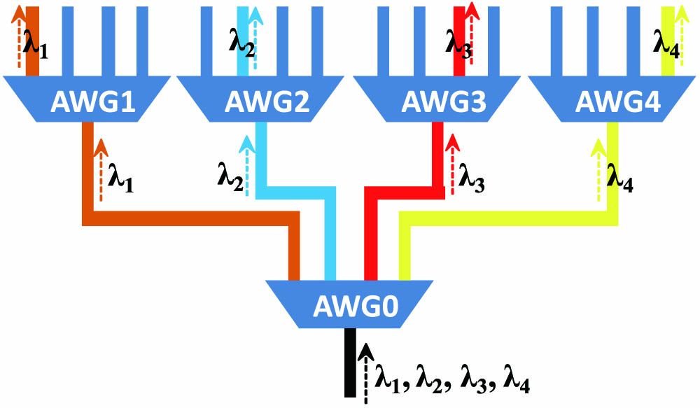
The schematic of the cascaded silicon photonics AWG is shown in Fig. 1. The five AWGs (from AWG0 to AWG4) have the same design. Table 1 shows the main design parameters of a single AWG. The AWG is designed for a channel spacing of 6.4 nm at 1550 nm. In order to reduce the coupling loss between the nanotaper and the optical lensed fiber at the input while ensuring mode confinement at the output, the ridge waveguides are gradually transited into channel waveguides at the input/output of the AWG. The channel waveguides are 500 nm wide and 220 nm tall. The ridge waveguides are adopted as arrayed waveguides in order to reduce the phase error caused by the fabrication. The width of the arrayed waveguide is 600 nm, and it has a slab thickness is 120 nm, which is designed for single-mode transmission in the arrayed waveguide. The device is designed to operate at the grating order of 28, with a path length difference of 13.95 μm for the transverse-electric (TE) mode. The free propagation region (FPR) focal length is 82.9 μm. The minimum pitch between the neighboring waveguides is 2.5 μm at the fan-out section. The minimum radius of the arrayed waveguide is 30 μm. The number of arrayed waveguides is 20. The free spectrum range (FSR) is 44.1 nm. The operation is shown below. Four wavelength signals, , are launched into the input waveguide of the first AWG (AWG0). The four signals are separately coupled into the four output channels of AWG0, shown in Fig. 1. After AWG0, the four signals, , are separately coupled into . After further filtering, come out separately from the first output waveguide of AWG1, the second output waveguide of AWG2, the third output waveguide of AWG3, and the fourth output waveguide of AWG4, respectively. In principle, no signal will come out from the other output waveguide of . However, some weak signals will come out from these other output waveguides, due to the crosstalk. In order to compare the crosstalk improvements of the cascaded AWGs, we also design one single AWG, the layout of which is the same as the others.
| Silicon waveguide total height | 220 nm |
| Silicon rib waveguide height | 120 nm |
| Min. pitch of input/output waveguides | 2.5 μm |
| Min. pitch of arrayed waveguides | 2.5 μm |
| Width of arrayed waveguides | 600 nm |
| Channel spacing | 6.4 nm |
| Grating order | 28 |
| FPR | 82.9 μm |
| FSR | 44.1 nm |
| Number of arrayed waveguide | 20 |
| Min. radius of arrayed waveguides | 30 μm |
| Length difference of arrayed waveguides | 13.95 μm |
| Operation wavelength | 1.55 μm |
Table 1. Design Parameters of a Single AWG

Figure 1.Schematic of cascaded silicon photonics AWG.
The device was fabricated on an 8-inch SOI wafer with a 220-nm-thick top silicon layer and a 2-μm-thick buried oxide layer using 248-nm-deep UV lithography. A 60-nm-thick layer was first deposited as a hard-mask layer for the silicon etching process. After the first lithography, the hard-mask oxide was etched by reactive ion etching to form the waveguide pattern on the oxide layer. Then, the photoresist was stripped, and the wafer was cleaned using hydrofluoric and an sulfuric peroxide mixture solution. After cleaning, the top silicon layer was partially etched using an Applied Materials Precision 5000 Etcher, and the remaining silicon height was 120 nm. The second lithography was processed for the waveguide formation, and the remaining silicon was fully etched to BOX to form the waveguide. Finally, a more than 100-μm-deep trench was etched for fiber coupling. This deep trench is very useful to reduce the coupling loss with input/output fibers instead of polishing the device. The scanning electron microscope (SEM) images are shown in Fig. 2, and the transmission electron microscope (TEM) result of one of the arrayed waveguides is shown in Fig. 3. Figure 2(a) is the fan-out range of the AWG. The minimum gap between the arrayed waveguides is only 200 nm wide for reducing the transmission loss of the AWG. Figure 2(b) is the deep trench, which is more than 100 μm deep. The image in Fig. 2(c) is the nanotip, which is 200 nm wide. The nano tip is located near the deep trench, and the 1-μm-wide gap between the nanotip and the deep trench is designed for avoiding the misalignment of the deep-trench lithography. Figure 2(d) is the transition area from the rib waveguide to the channel waveguide. This transition structure is usually used to reduce the optical transition loss between channel waveguides and rib waveguides. The measured slab thickness of the arrayed waveguide is 115 nm, close to the design value of 120 nm. The measured total Si thickness is around 216 nm, also close to the design value of 220 nm. However, the final waveguide width is only 550 nm. The optical microscope image of the device after fabrication is shown in Fig. 4. The size of the silicon cascaded AWG is . The core size of a single AWG is .
Figure 2.SEM images of cascaded silicon photonics AWG.
Figure 3.TEM image of one arrayed waveguide.
Figure 4.Optical microscope image of cascaded arrayed waveguides.
After dicing, the chip was measured using a high-performance amplified spontaneous emission light source with broadband wavelengths, a polarization controller, an optical polarizer, a high-sensitivity optical power meter, and a high-precision optical spectrum analyzer. The TE mode of the input light was operated by a polarizer. Then, we measured the optical spectrum of the input polarization-maintaining (PM) lensed fiber to the output PM lensed fiber. Later, the TE spectra of the silicon cascaded AWG and the reference single AWG were achieved using the same characterization. The spectra are shown in Figs. 5 and 6. The main results are shown in Table 2. By the characterization of the cutback channel/ridge waveguides, the measured propagation losses of the channel waveguide and the ridge waveguide are 2.0 and 1.6 dB/cm, respectively. Based on the propagation loss, the fiber-to-waveguide coupling loss of 1.8 dB/facet is achieved. By deducting the coupling loss, we estimate the on-chip transmission loss of the single AWG to be 2.0 dB, and the on-chip transmission loss of the cascaded AWGs is about 4.0 dB. In order to reduce the loss of the AWG, it is necessary to reduce the propagation loss of the silicon waveguide and to improve the resolution of the lithography for a smaller minimum gap between the arrayed waveguides. The loss non-uniformity of the cascaded AWGs is 0.4 dB, which is twice as large as that of the single AWG. The crosstalk has been dramatically improved. The crosstalk of the cascaded AWGs is only . Compared to the single AWG (its crosstalk is ), a crosstalk of more than 20 dB is obtained. According to the measured waveguide propagation loss, the scattering effect of the nanowire silicon waveguide resulting from the waveguide roughness should be obvious. This effect is one factor of the high crosstalk of a single AWG. At the same time, silicon photonics AWGs are very sensitive to the phase errors. The phase errors from the design and fabrication further cause the crosstalk of the single AWG. The channel spacings for both AWGs are close to the design value of 6.4 nm.
| | Single AWG | Cascaded AWG |
|---|
| Insertion loss (including coupling loss of 3.6 dB) | 5.6 dB | 7.6 dB |
| Loss non-uniformity | 0.2 dB | 0.4 dB |
| Crosstalk | 12.5 dB | 33.2 dB |
| 1st channel wavelength (λ1) | 1569.2 nm | 1570.2 nm |
| 2nd channel wavelength (λ2) | 1575.6 nm | 1576.6 nm |
| 3rd channel wavelength (λ3) | 1581.9 nm | 1582.9 nm |
| 4th channel wavelength (λ4) | 1588.2 nm | 1589.3 nm |
| Channel spacing | 6.4±0.1 nm | 6.4±0.1 nm |
| FSR | 44.5 nm | 44.5 nm |
| Average 3-dB bandwidth | 3.0 nm | 1.9 nm |
Table 2. Results of Single AWG and 1×4 Cascaded AWGs
Figure 5.Spectrum of the single AWG (TE).
Figure 6.Spectrum of cascaded arrayed waveguides (TE).
Due to the fabrication deviation and testing environment difference, the central wavelength shifts more than 20 nm to the long wavelength direction, compared to the design. The measured wavelength of each channel of both AWGs shows the wavelength difference of the corresponding channel is only 1 nm. Both AWGs are fabricated on the same die of the same wafer. So, the result also proves that the fabrication uniformity is good. After being filtered twice, the 3-dB bandwidth of the cascaded AWGs become smaller: it is 60% of the single AWG.
In conclusion, a 4-channel cascaded silicon photonics AWG is fabricated on an SOI platform. The silicon thickness of the SOI wafer is 220 nm. The on-chip transmission loss of the single AWG is 2.0 dB, and the fiber-to-waveguide coupling loss is 1.8 dB/facet. The on-chip transmission loss of the cascaded AWGs is around 4.0 dB. The measured channel spacing is , close to the design value of 6.4 nm. The cascaded AWGs have a good crosstalk of . Compared to the single AWG, the design of the cascaded structure improves the crosstalk by more than 20 dB. After being filtered twice, the cascaded AWG has a small 3-dB bandwidth and a little high loss non-uniformity. This solution is a good choice to resolve the issue of the crosstalk of AWGs fabricated on SOI wafers with a thin top silicon layer, although the on-chip transmission loss will increase. Once the waveguide propagation loss can be further improved, the on-chip loss of the cascaded AWG will be reduced.
References
[1] J.-X. Cai, K.-M. Feng, A. E. Willner, V. Grubsky, D. S. Starodubov, J. Feinberg. IEEE Photon. Technol. Lett., 11, 1455(1999).
[2] J. F. Song, Q. Fang, T.-Y. Liow, H. Cai, M. B. Yu, G. Q. Lo, D.-L. Kwong, JthA020(2011).
[3] J. Brouchaert, W. Bogaerts, S. Selvaraja, P. Dumon, R. Baets, D. V. Thourhout. IEEE Photon. Technol. Lett., 20, 309(2008).
[4] S. Kamei, T. Shibata, Y. Inoue. IEEE Photon. Technol. Lett., 21, 1695(2009).
[5] L. Jia, M. Geng, L. Zhang, L. Yang, P. Chen, Y. Liu. Chin. Opt. Lett., 8, 485(2010).
[6] X. Feng, Z. Wu, X. Wang, S. He, S. Gao. Photon. Res., 4, 245(2016).
[7] S. Zhao, L. Lu, L. Zhou, D. Li, Z. Guo, J. Chen. Photon. Res., 4, 202(2016).
[8] K. Jia, J. Yang, Y. Hao, X. Jiang, M. Wang, W. Wang, Y. Wu, Y. Wang. IEEE J. Sel. Top. Quantum Electron., 12, 1329(2006).
[9] Q. Fang, J. F. Song, G. Zhang, M. B. Yu, Y. L. Liu, G. Q. Lo, D.-L. Kwong. IEEE Photon. Technol. Lett., 21, 319(2009).
[10] Q. Fang, J. F. Song, X. S. Luo, X. G. Tu, L. X. Jia, M. B. Yu, G. Q. Lo. IEEE Photon. Technol. Lett., 28, 2533(2016).
[11] J. F. Song, Q. Fang, S. H. Tao, M. B. Yu, G. Q. Lo, D.-L. Kwong. IEEE Photon. Technol. Lett., 20, 2156(2008).
[12] L. Yang, J. F. Ding. J. Lightwave Technol., 32, 966(2014).
[13] H. Chen, P. Verheyen, P. H. De, G. Lepage, J. C. De, S. Balakrishnan, P. Absil, W. Yao, L. Shen, G. Roelkens, J. C. Van. Opt. Express, 24, 4622(2016).
[14] W. Bogaerts, P. Dumon, D. V. Thourhout, D. Taillaert, P. Jaenen, J. Wouters, S. Beckx, V. Wiaux, G. R. Baets. IEEE J. Sel. Top. Quantum Electron., 12, 1394(2006).
[15] S. Pathak, M. Vanslembrouck, P. Dumon, D. V. Thourhout, W. Bogaerts. J. Lightwave Technol., 31, 87(2013).
[16] L. Wang, W. Bogaerts, P. Dumon, S. K. Selvaraja, J. Teng, S. Pathak, X. Han, J. Wang, X. Jian, M. Zhao, R. Baets, G. Morthier. App. Opt., 51, 1251(2012).
[17] Q. Fang, T.-Y. Liow, J. F. Song, K. W. Ang, M. B. Yu, G. Q. Lo, D.-L. Kwong. Opt. Express, 18, 5106(2010).
[18] H. L. W. Gao, E. Li, C. Tang. IEEE Photon. J., 7, 7802707(2015).