Abstract
Enhancing light–matter interaction in cavity quantum electrodynamics has aroused widespread interests in on-chip quantum information processing. Here, we propose a hybrid nanotoroid–nanowire system to enhance photon–exciton interaction. A nanoscale gap is formed by placing a dielectric nanowire close to a dielectric nanotoroid, where the coupling coefficient between photon and emitter can achieve 5.55 times of that without nanogap. Meanwhile, the cavity loss and spontaneous emission of the emitter will remain at a small value to guarantee the realization of strong coupling. The method might hold promise for the research of nanophotonics, quantum optics, and novel optical devices.Cavity quantum electrodynamics (CQED) aims to study the quantum behaviors of light–matter interaction at the single photon level[1–5]. Recently, tailoring the interaction between atoms and the electromagnetic field at the sub-wavelength scale in the strong coupling regime has already been crucial to a wide range of applications, like single photon sources[6,7], superconductors[8], and quantum gates[9,10]. The condition to realize the strong coupling between a quantum emitter and cavity photons is , [11,12], where refers to the interaction strength between the emitter and cavity modes, is the cavity loss rate, and is the spontaneous emission rate of the emitter. Hence, it is of great importance to enhance the coupling coefficient while restraining and at relatively small values to achieve strong coupling in nanocavities. In previous studies, great efforts have been made in the areas of Fabry–Perot optical cavities[13,14], surface plasmon cavities[15,16], and photonic crystal cavities[17], both theoretically and experimentally to meet the requirements of strong coupling.
Among the most known types of cavities, whispering gallery modes (WGMs) cavities are with high-profile because the combination of their ultrahigh quality factor and ultrasmall mode volume makes them promising candidates for the study of CQED[18–21]. So far, numerous microstructures, such as microsphere[22] and microdisk resonators[23], have been proposed to achieve strong coupling based on WGMs, where the coupling coefficient is usually several hundred megahertz (MHz) in microstructures of a few microns[24]. Furthermore, nanogap structures can confine light at the nanoscale, thus enhancing electric field intensity dramatically[25], which makes it of fundamental importance in CQED. In previous studies, researchers have taken use of nanogap structures to achieve large spontaneous emission[26,27] and large reversible photon–exciton interaction enhancement[28,29]. However, the proposal of reaching strong coupling in a nanogap while restraining the cavity loss observably under the effect of WGMs has not been reported.
Here, combining the advantages of strong local field enhancement in the nanogap with high quality factor of WGMs, strong coupling in low loss optical cavities can be realized. We demonstrate theoretically a hybrid nanotoroid–nanowire system with a nanogap that can achieve large photon–exciton coupling, meanwhile maintaining low cavity loss and weak spontaneous emission. Under the excitation of the source, a hot spot appears within the nanogap, which leads the coupling coefficient enhanced by several times [about several hundred gigahertz (GHz)]. It is worth mentioning that the cavity loss and the spontaneous emission are maintained at small values in these processes ( about one hundred GHz and about several hundred MHz), which are far less than , so that a strong coupling condition can be easily achieved. By carefully adjusting the dielectric constant of the nanostructures, the radius of the nanotoroid, or the width of the nanogap, the coupling coefficient can be modulated within a few hundred GHz, realizing wide-range modulation. The cavity loss rate is at least two orders of magnitude smaller than that of surface plasmon nanocavities[28], and the coupling coefficient can reach an order of several hundred GHz, significantly higher than that of WGMs with dimensions of microns[24]. Not limited within present toriodal nanostructures, the idea of this work can be extended to other custom-designed shapes like nanospheres or nanopolygons. This model will provide a method to study strong coupling in low loss cavities and promote the development of on-chip quantum information processing.
Sign up for Chinese Optics Letters TOC. Get the latest issue of Chinese Optics Letters delivered right to you!Sign up now
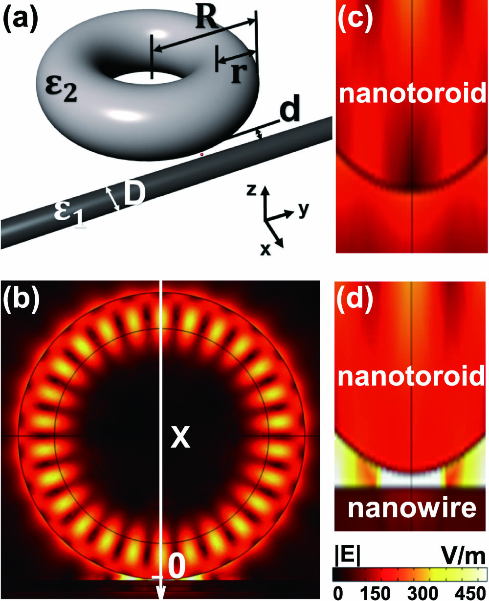
A dielectric nanotoroid is an ideal platform to support WGMs, which has already been used to implement multiple functionalities, such as sensing[30], lasing[31], and strong coupling[32]. Meanwhile, dielectric nanowires can transmit evanescent wave modes. Compared with a metal nanowire, it has advantages in respect to low loss transmission. A nanoscale gap can be formed by bring the two nanostructures mentioned above together, integrating the advantages of low cavity loss and localized field enhancement. Figure 1(a) shows the diagram of the nanotoroid–nanowire system schematically; a dielectric nanotoroid with major radius and minor radius is coupled to a dielectric nanowire, thus forming a nanoscale gap. Parameter expresses the width of the gap. The dielectric constants of the nanowire and the nanotoroid are represented as and , respectively. A two-level quantum emitter polarized along the X axis, like an atom, molecule, or quantum dot, can be inserted into the gap. The dimensions of the nanowire are comparable with the nanotoroid. WGMs of the nanotoroid and evanescent wave modes of the nanowire can couple with each other and form gap modes; here, we identify the coupled modes as cavity modes, and strong photon–exciton interaction can occur within the nanogap.

Figure 1.Nanotoroid–nanowire system. (a) Schematic diagram of a dielectric nanotoroid close to a dielectric nanowire. (b) Electric field distribution of the nanostructure. Details of electric field distributions of the same size nanotoroid (c) without and (d) with nanowire with parameters , , , , , , and working wavelength .
In order to compute the photon–exciton coupling coefficient , the cavity loss , and the spontaneous emission rate of the emitter, we resort to three-dimensional numerical simulations by commercial COMSOL multiphysics software. We build a cylindrical model in COMSOL. The radius and the length of this model are 3 μm and 10 μm, respectively, much bigger than those of the nanowire and the nanotoroid (about several hundred nanometers). Meanwhile, a perfectly matched layer is introduced to minimize boundary reflections. In this instance, computed results are almost constant (less than one percent change) when changing the sizes of the boundary or the length of the nanowire, so our model can simulate an infinite environment.
In the following discussion, a specific example is taken into account, the major radius and minor radius of the toroid are set to and , respectively, with the dielectric constant of . A dielectric nanowire with diameter of 100 nm and dielectric constant of is placed away from the nanotoroid. Here, the dipole moment of the quantum emitter is set as .
The related parameters , , and in this coupled nanotoroid–nanowire system can be solved by the following algorithm. The coupling coefficient expresses the interaction strength between the emitter and the cavity, which is defined as [33], where denotes the transition dipole moment and is set as a constant. is the electric field of single photon excitation that is normalized by photons, is the total energy of the cavity modes and can be obtained by calculating the integral of the energy surrounding the cavity, and is the electric field intensity that is obtained directly through COMSOL simulation. The photon loss rate through the cavity can be obtained from the full width at half-maximum (FWHM) of the normalized energy of the cavity modes spectra[28]. Another loss that needs to be addressed is the photons emission to the far field rather than cavity modes, which can be calculated indirectly in the form of [25]. A nanosphere with a radius of 1 nm wrapping the emitter is used to calculate the total power of the emitter without a nanowire by surface integrals over the Poynting vector on the sphere. The far field radiation power is the surface integral over the Poynting vector on the whole flank of the model that is regarded as far field with the coupled system. Spontaneous emission rate in vacuum is a constant of under certain parameters[34]. Thus, we can obtain the parameters , , and by the method mentioned above.
Adjusting the wavelength of the light source, we can stimulate WGMs of the nanotoroid at . The corresponding electric field distribution is shown in Fig. 1(b). It becomes unsymmetrical surrounding the nanotoroid on account of the existence of the nanowire. By comparing the electric field distributions of the same size nanotoroid without [Fig. 1(c)] and with [Fig. 1(d)] the nanowire, we can obviously find that there is a hot spot in the nanogap between two nanostructures, which will be in favor of enhancing the photon–exciton coupling.
The coupling strength within the nanogap in the hybrid nanotoroid–nanowire system can be enhanced by several times compared with that of the no nanowire structure. Figure 2(a) shows the variation of the coupling coefficient along the X axis for both with (the red curve) and without (the blue curve) the dielectric nanowire. The outer edge of the nanotoroid is set as the origin of the horizontal axis [shown in Fig. 1(b)]. With the dielectric nanowire, the coupling coefficient can reach its maximal value at the boundary between the nanowire and the nanogap, while without the nanowire at the same position. The coupling coefficient at the nanogap achieves 5.55 times enhancement. The reason for this enhancement is that as the cavity size is reduced, a reduction of mode volume will occur, followed by a large confinement of the electromagnetic field. Compared with previous studies, the coupling coefficient in an individual dielectric toroid with a radius of several microns is generally in the order of hundreds of MHz, much smaller than the value of our research[24]. Thus, we can draw the conclusion that within the nanogap of the hybrid nanostructure, the photon–exciton coupling can be enhanced dramatically.
Figure 2.Mechanism of enhancing the coupling coefficient and maintaining comparatively low cavity loss . (a) The variation of the coupling coefficient along the X axis. with nanowire and without nanowire, respectively. (b) The variation of the normalized energy of the cavity modes with the wavelength . with nanowire and without nanowire, respectively.
The feature of low cavity loss of WGMs is almost unaffected when the dielectric nanowire exists, which is a favorable characteristic of our research. As shown in Fig. 2(b), the red and blue curves represent the normalized energies of the cavity modes with and without the nanowire, respectively, by integrating the energy density around the nanocavity with the parameters mentioned above. The cavity loss can be calculated through the FWHM of the spectra. For the same size nanotoroid, resonant wavelength with a nanowire has a slight shift (less than 0.1 nm) in comparison to that without it. The FWHM of the red curve indicates , only a little higher than that of the blue curve with , illustrating that the nanowire introduces additional loss, which is too small to break the strong coupling condition. Another loss that needs to be addressed is the photons emitting to free space rather than cavity modes. It is found that in our structure, the spontaneous emission is only hundreds of MHz, while and are at the GHz level. So, it is reasonable to take no account of the spontaneous emission . Previous studies have also shown that is weak enough to be ignored compared with other radiation channels[25]. In short, , in the nanogap of our nanotoroid–nanowire system, reaching strong coupling condition.
The enhancement of the coupling coefficient comes from the ultrasmall mode volume of the nanogap structures, which is affected by the dielectric constant of the nanowire and of the nanotoroid. First, we investigate the variation of the coupling coefficient with the dielectric constant of nanowires ranging from 7 to 12. As shown in Fig. 3(a), for different minor radii of the nanotoroid and , respectively, we can see that the coupling strength in the cavity can be enhanced observably with increasing dielectric constant of the nanowire. Then, the calculated coupling coefficient for the nanocavity versus dielectric constant of the nanotoroid is shown in Fig. 3(b), which reveals that the higher can also lead to the stronger photon–exciton coupling in our hybrid nanostructure. These tendencies are direct results of the reduction of the mode volume , owing to the increment of the dielectric constant, which agrees well with previous research[19].
Figure 3.Results of the coupling coefficient influenced by relevant parameters. (a), (b) increases with the growth of and . (c) increases with the shortening of .
The mode volume of the cavity can be strongly influenced by the size of the nanogap. As far as our hybrid nanocavity, a convenient method is to alter the width of the nanogap by controlling the spatial position of the nanowire. As shown in Fig. 3(c), for both and , the coupling coefficients increase with the width of the nanogap narrowing from 10 to 2 nm. This rule enlightens us to the fact that narrowing the gap in our model can reach more effective coupling between the light and the emitter. The calculations also show an increment of the coupling coefficient , as the nanotoroid minor radius is decreased by comparing the two curves in each figure. These increments are caused by the depressed optical mode volume and the increasing confinement of field as the width of the nanogap or the minor radius of the nanotoroid is reduced. Considering the balance between the desired large coupling coefficient and the difficulty of the experiment, we present the results at in the main result. Moreover, corresponding and are almost unaffected and remain at relatively small values in the above models, which guarantee the realization of strong coupling.
We also use Ag nanowire to replace the dielectric nanowire to explore the photon–exciton coupling in the dielectric-nanotoroid–metal-nanowire coupled system. Ag nanowire can support a surface plasmon polariton. When it is in close proximity to a dielectric nanotoroid, gap modes will appear between two nanostructures under the influence of a surface plasmon polariton and WGMs. The electric field distribution is displayed in the inset of Fig. 4(a), where the parameters are the same as above except the dielectric nanowire is replaced by Ag nanowire. Obviously, there is also a hot spot within the nanogap. Figure 4(a) shows the variation of the coupling coefficient along the X axis. Compared to other positions, in the nanogap is enhanced significantly, and reaches its maximum at the interface of the nanogap and the nanowire. However, the inherent loss of the metal will have a great influence on the parameter , which requires our attention. The cavity loss can be calculated as by measuring the FWHM of the spectra in Fig. 4(b), which is about 70 times that in the nanotoroid–dielectric-nanowire structure with same size. Therefore, in the nanotoroid–metal-nanowire system, indicating that the emitter loses its energy through the cavity principally rather than interacting with the cavity modes, which does not meet the demand of the strong coupling.
Figure 4.Results of coupling coefficient and cavity loss in the nanotoroid–Ag-nanowire system. (a) The variation of the coupling coefficient along the X axis. At the interface of the nanogap and the nanowire, the coupling coefficient can reach its maximum . Inset in (a) shows the electric field distributions of the WGMs of the nanotoroid and the surface plasmon polariton of the nanowire. (b) Normalized energy of the cavity modes changes with wavelength . with Ag nanowire.
With currently available nanotechnologies, the spatial position of individual nanowires and other nanostructures can be controlled accurately. A nanoscale gap can be formed experimentally[29,35–37]. Particularly, in Ref. [29], researchers have achieved a nanogap with experimentally, so our scheme has the possibility of being experimentally implemented and is expected to achieve strong coupling in the low loss cavity of nanometer magnitude.
In conclusion, we have theoretically demonstrated a hybrid nanotoroid–dielectric-nanowire structure supporting gap modes to enhance photon–exciton coupling, which can combine the advantages of strong local field enhancement of the nanogap structure with low cavity loss of the WGMs. The coupling coefficient between the photon and emitter can achieve 5.55 times enhancement within the nanogap. In our model, increasing the dielectric constant of each nanostructure, narrowing the width of gap, or shrinking the radius of the nanotoroid can effectively enhance the coupling coefficient , while introducing a metal nanowire will bring enormous cavity loss that destroys the strong coupling condition. Our method to reach strong coupling in a low loss nanocavity is helpful to subsequent researches, such as state manipulation, entanglement, and quantum gates. Furthermore, enhancing light–matter interaction at the sub-wavelength scale will open new opportunities for on-chip photonics circuits and quantum information technologies.
References
[1] K. J. Vahala. Nature, 424, 839(2003).
[2] J.-M. Pirkkalainen, S. U. Cho, J. Li, G. S. Paraoanu, P. J. Hakonen, M. A. Sillanpaa. Nature, 494, 211(2013).
[3] H. Mabuchi, A. C. Doherty. Science, 298, 1372(2002).
[4] H. J. Kimble. Phys. Scr. T, T76, 127(1998).
[5] X. L. Zhong, G. W. Lin, F. X. Feng, Y. P. Niu, S. Q. Gong. Chin. Opt. Lett., 13, 092701(2015).
[6] B. Lounis, M. Orrit. Rep. Prog. Phys., 68, 1129(2005).
[7] J. Su, L. Cui, Y. H. Li, X. Y. Li. Chin. Opt. Lett., 16, 041903(2018).
[8] A. Blais, A. M. van den Brink, A. M. Zagoskin. Phys. Rev. Lett., 90, 127901(2003).
[9] M. S. Zubairy, M. Kim, M. O. Scully. Phys. Rev. A, 68, 033820(2003).
[10] R. T. Zhao, R. S. Liang. Chin. Opt. Lett., 14, 062701(2016).
[11] O. Benson. Nature, 480, 193(2011).
[12] M. S. Tame, K. R. McEnery, S. K. Ozdemir, J. Lee, S. A. Maier, M. S. Kim. Nat. Phys., 9, 329(2013).
[13] C. J. Hood, T. W. Lynn, A. C. Doherty, A. S. Parkins, H. J. Kimble. Science, 287, 1447(2000).
[14] J. M. Gerard, B. Sermage, B. Gayral, B. Legrand, E. Costard, V. Thierry-Mieg. Phys. Rev. Lett., 81, 1110(1998).
[15] D. E. Chang, A. S. Sorensen, P. R. Hemmer, M. D. Lukin. Phys. Rev. Lett., 97, 053002(2006).
[16] N. P. de Leon, B. J. Shields, C. L. Yu, D. E. Englund, A. V. Akimov, M. D. Lukin, H. Park. Phys. Rev. Lett., 108, 226803(2012).
[17] K. Srinivasan, P. E. Barclay, O. Painter, J. X. Chen, A. Y. Cho, C. Gmachl. Appl. Phys. Lett., 83, 1915(2003).
[18] D. K. Armani, T. J. Kippenberg, S. M. Spillane, K. J. Vahala. Nature, 421, 925(2003).
[19] S. M. Spillane, T. J. Kippenberg, K. J. Vahala. Phys. Rev. A, 71, 013817(2005).
[20] M. L. Gorodetsky, A. A. Savchenkov, V. S. Ilchenko. Opt. Lett., 21, 453(1996).
[21] D. W. Vernooy, A. Furusawa, N. P. Georgiades, V. S. Ilchenko, H. J. Kimble. Phys. Rev. A, 57, R2293(1998).
[22] Y.-S. Park, A. K. Cook, H. Wang. Nano Lett., 6, 2075(2006).
[23] Y. F. Xiao, C. L. Zou, P. Xue, L. X. Xiao, Y. Li, C. H. Dong. Phys. Rev. A, 81, 053807(2010).
[24] J. R. Buck, H. J. Kimble. Phys. Rev. A, 67, 033806(2003).
[25] H. Lian, Y. Gu, J. J. Ren, F. Zhang, L. J. Wang, Q. H. Gong. Phys. Rev. Lett., 114, 193002(2015).
[26] K. J. Russell, T.-L. Liu, S. Cui, E. L. Hu. Nat. Photon., 6, 459(2012).
[27] X. K. Duan, J. J. Ren, F. Zhang, H. Hao, G. W. Lu, Q. H. Gong, Y. Gu. Nanotechnology, 29, 045203(2018).
[28] J. J. Ren, Y. Gu, D. X. Zhao, F. Zhang, T. C. Zhang, Q. H. Gong. Phys. Rev. Lett., 118, 073604(2017).
[29] R. Chikkaraddy, B. de Nijs, F. Benz, S. J. Barrow, O. A. Scherman, E. Rosta, A. Demetriadou, P. Fox, O. Hess, J. J. Baumberg. Nature, 535, 127(2016).
[30] B. B. Li, Y. F. Xiao, C. L. Zou, Y. C. Liu, X. F. Jiang, Y. L. Chen, Y. Li, Q. H. Gong. Appl. Phys. Lett., 98, 021116(2011).
[31] S. L. McCall, A. F. J. Levi, R. E. Slusher, S. J. Pearton, R. A. Logan. Appl. Phys. Lett., 60, 289(1992).
[32] Y. F. Xiao, Y. C. Liu, B. B. Li, Y. L. Chen, Y. Li, Q. H. Gong. Phys. Rev. A, 85, 031805(2012).
[33] H. Raether. Surface Plasmons on Smooth and Rough Surfaces and on Gratings(1986).
[34] M. O. Scully, M. S. Zubairy. Quantum Optics(2000).
[35] G. M. Akselrod, C. Argyropoulos, T. B. Hoang, C. Ciraci, C. Fang, J. Huang, D. R. Smith, M. H. Mikkelsen. Nat. Photon., 8, 835(2014).
[36] J. B. Lassiter, F. McGuire, J. J. Mock, C. Ciraci, R. T. Hill, B. J. Wiley, A. Chilkoti, D. R. Smith. Nano Lett., 13, 5866(2013).
[37] D. O. Sigle, J. T. Hugall, S. Ithurria, B. Dubertret, J. J. Baumberg. Phys. Rev. Lett., 113, 087402(2014).