W. C. Dong1, J. Hou1, Y. S. Kadhim2, S. K. Tawfeeq2, and X. L. Zhang1,*
Abstract
All-optical canonical logic units at 40 Gb/s using bidirectional four-wave mixing (FWM) in highly nonlinear fiber are proposed and experimentally demonstrated. Clear temporal waveforms and correct pattern streams are successfully observed in the experiment. This scheme can reduce the amount of nonlinear devices and enlarge the computing capacity compared with general ones. The numerical simulations are made to analyze the relationship between the FWM efficiency and the position of two interactional signals.1. INTRODUCTION
All-optical logic operation is one of the basic signal processing functions, and has attracted intense attention in recent years. Various logic operation schemes have been proposed based on different nonlinear effects, such as cross-gain modulation [1], cross-phase modulation (XPM) [2], and four-wave mixing (FWM) [3]. Among them, the FWM effect has been widely investigated due to the advantages of femtosecond response time and modulation format transparency. FWM-effect-based reconfigurable exclusive or (XOR) and exclusive nor (XNOR) logic gates for 10 Gb/s nonreturn-to-zero polarization shift keying (NRZ-PolSK) signals have been realized [4]. By introducing the bidirectional FWM in a single highly nonlinear fiber (HNLF), 40 Gb/s XOR and XNOR logic gates are simultaneously realized theoretically [5]. However, to our best knowledge, no further experimental result has been demonstrated.
Apart from the above-mentioned basic computing operations, optical digital computing circuits with higher reconfigurability and versatility have also been well developed. A 0.5 Gb/s reconfigurable logic array is demonstrated by tuning the resonance wavelength of the microring resonator [6]. However, the speed limitation is difficult to break through since electrical-to-optical conversion is still required in these approaches. To overcome the speed bottleneck, an all-optical expanded programmable logic array (PLA) based on multi-input/output canonical logic units (CLUs) was designed using FWM in HNLF at 40 Gb/s [7], where two-input and three-input CLUs are simultaneously achieved in five parallel channels, and thus the computing capacity is comparatively larger than that of a standard one [1].
In this paper, CLUs of two 40 Gb/s inputs are proposed and demonstrated. Two minterms are simultaneously obtained by using the bidirectional FWM in a single HNLF, and other all- optical logic gates (XOR, XNOR, and all the maxterms) are further demonstrated by coupling specific minterms or original signals together. After introducing the experimental process, the relationship between the FWM efficiency and the position of two interactional signals is analyzed through numerical simulation. In short, this scheme has two prominent advantages: reducing the amount of nonlinear devices and enlarging the computing capacity. In addition, taking advantage of the femtosecond response time and modulation format transparency of FWM, the proposed scheme has the potential to achieve ultrahigh speed, up to the Tb/s level [8]. Thus, this scheme-based PLA is promising and the detail is discussed in the last part of the paper.
Sign up for Photonics Research TOC. Get the latest issue of Photonics Research delivered right to you!Sign up now
2. OPERATIONAL PRINCIPLE
In this section, the operational principle of the proposed scheme is presented. As Fig. 1 shows, the delayed interferometer (DI) is an asymmetric Mach–Zehnder interferometer with a differential delay in one arm and a tunable phase difference in the other. The transmission spectrum of the DI is comb-like. The differential phase shift keying (DPSK) signal passes through a DI with equaling the single-bit period, and two adjacent bits interfere with each other at two outputs, producing a pair of absolute and complementary codes. Therefore, the demodulation process of the DPSK signal can be regarded as a precoding process and makes the scheme more flexible to realize the CLUs.
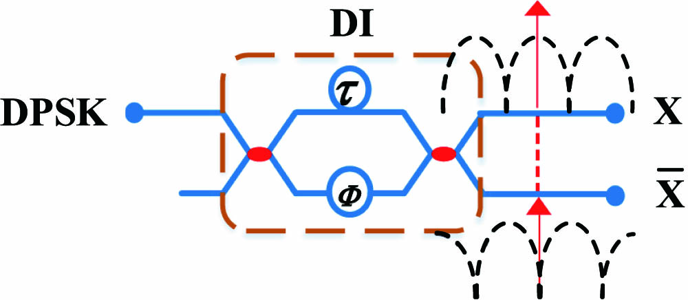
Figure 1.Operational principle of DI modulation.
The operational principle of minterm generation is shown in Fig. 2. Two NRZ-DPSK signals at different wavelengths can be demodulated by DIs to , , , and . After that, is coupled with while is coupled with and then injected into two ports of the HNLF, respectively. For the group of and , FWM between these data streams generates two idlers at wavelengths of (idler1) and (idler2), respectively. The intensity of idler1 (2) is proportional to the intensity product of the signal at () and the square of the signal at (). Therefore, the idlers will carry the logic “1” state if both input data are at a state of “1”, while the logic state will be “0” if one of the input signals carries the logic “0” state, corresponding to a CLU of . Thus, can be simultaneously achieved in two parallel channels, i.e., idler1 and idler2. In the other direction, a CLU of is simultaneously obtained at the same wavelength as . The rest of the CLUs, i.e., and , are realized simultaneously in the same way after exchanging the outputs of and , as shown in Fig. 2.

Figure 2.Operational principle of the proposed scheme.
It is known that the XOR and XNOR operations can be expressed by the formulas and , respectively. After coupling the two outputs of HNLF, the idlers are extracted by one bandpass filter at the wavelength of . Then, the XNOR () or XOR () logic gate is realized. In addition, the four maxterms can be calculated by the formulas , , , and . Thus, the four maxterms are generated through simply coupling the specific minterms with the corresponding original signals. These obtained logic gates, except for XOR and XNOR, constitute the CLUs for the two-input system.
It is worth mentioning that the FWM and XPM induced by the counterpropagating signals can be negligible because of the walk-off effect, and our experiment demonstrates that crosstalk is not serious.
3. EXPERIMENTAL RESULTS AND DISCUSSION
As Fig. 3 shows, two 40 Gb/s NRZ-DPSK signals with a pseudo-random binary sequence (PRBS) at wavelengths of 1551.3 nm () and 1549.7 nm () are generated by the transmitter (Tx). Then, an arrayed waveguide grating with a free-spectral range (FSR) of 1.6 nm is utilized to demultiplex the two signals, which have been amplified to 14.5 dBm by the former erbium-doped fiber amplifier (EDFA). Afterward, the signals are launched into two DIs with a FSR of 40 GHz and demodulated to two couples of on–off keying (OOK) signals , and , acting as the original input signals for subsequent logic gates. Then, two optical delay lines (ODLs) are applied to decorrelate and with and signals.
Figure 3.Experimental setup for configurable multiple logic gate generation.
After passing through the polarization controllers (PCs), two couplets of different signals are injected into two ports of bidirectional HNLF. The average power of , measured before HNLF is 15.68 and 10.47 dBm, respectively. The nonlinear coefficient of the HNLF is with a zero dispersion wavelength of 1550 nm and dispersion slope of . The length is 1 km and the loss is 1.5 dB/km. To verify the efficiency of the FWM, the spectra right after the output of the HNLF was measured as shown in Fig. 4. An obvious FWM effect can be observed with two idlers at 1548.1 and 1552.9 nm, respectively. The idlers are extracted by a subsequent tunable bandpass filter with a 3 dB bandwidth of 0.8 nm. The is applied to synchronize the two minterms before coupling. After amplification by the EDFA, the output signals are monitored by the communication signal analyzer (CSA) as well as optical spectrum analyzer (OSA).
Figure 4.Measured spectra of FWM in the HNLF.
As shown in Fig. 5, the optical signal-to-noise ratios (OSNRs) of minterms in two parallel channels measured via OSA with a resolution of 0.1 nm are over 30 and 32 dB, respectively, reflecting a good performance of the logic results. The temporal waveforms of the original DPSK signal and demodulated signals are illustrated in Fig. 6(a) and show good output performance after the demodulation. However, the “1”s are not so flat due to the amplitude fluctuation of the original DPSK signals. The temporal waveforms of the minterms are illustrated in Fig. 6(b). One can see that the logic sequences of the minterms are correct with clear data streams, and the logic levels of the results can be clearly identified. Besides, the noise power is reduced due to the FWM gain saturation derived by pump depletion. The temporal waveforms of combinational logic functions are illustrated in Fig. 6(c). For the waveforms of XOR and XNOR the logic sequences are correct, with clear data streams. For the waveforms of maxterms, the “1”s are not so clearly identified mainly because of the amplitude fluctuation of the original DPSK signals. To achieve better performance of logic gates based on minterms, original signals with better quality are expected and synchronization of the minterms should be carefully optimized.
Figure 5.Measured OSNRs of minterms.
Figure 6.Measured temporal waveforms. (a) Original signals, (b) CLUs in HNLF, and (c) all combinational logic functions.
To make further analysis of the principle of the proposed scheme, we have provided numerical simulation results as shown in Fig. 7. In our simulation model, the parameters are set similar to the experimental HNLF. In addition, two continuous waves of the same power take the place of the modulated signals A and B. The relationships between the FWM efficiency, position of the two signals, and wavelength separation are investigated separately.
Figure 7.FWM efficiency comparison (a) when signal B is fixed at 1549.7 nm and (b) when the wavelength separation between signal A and signal B is fixed at 0.8, 1.6, and 2.4 nm, respectively.
In Fig. 7(a), the wavelength of signal B is fixed at 1549.7 nm, while the wavelength of signal A is changed from 1546.5 to 1552.9 nm by a step of 0.2 nm. It can be clearly seen that the FWM efficiency of signal idler1 is identical to signal idler2, while wavelength of signal A changes from 1548.1 to 1551.7 nm. In Fig. 7(b), when the wavelength separation between A and B is fixed at 0.8 nm, the shorter wavelength (wavelength of signal A) changes from 1546.5 to 1552.9 nm by a step of 0.8 nm and the wavelength of B changes correspondingly. One can see that the two change curves of the idlers almost overlap. When the wavelength separation increases to 1.6 nm, the FWM efficiency of idler1 is close to idler2 while signal A changes from 1548.1 to 1550.5 nm. In addition, with the wavelength separation increasing to 2.4 nm, the two change curves are uneven. In this case, the FWM efficiency is relatively high as long as the pump signal’s wavelength is close to the zero dispersion wavelength of the HNLF; otherwise, the efficiency drops rapidly. Therefore, in order to make a tradeoff between the crosstalk and the FWM efficiency, the experimental wavelengths are set at 1549.7 and 1551.3 nm, respectively.
For the application based on the proposed scheme, a bidirectional propagated waveguide-based PLA will be manufactured in the future. As we know, in a general CLU-PLA scheme [1] as shown in Fig. 8(a), CLUs with the same logic value are defined as a word line and the complete set of CLUs are defined as a bit line. Thus, as to an -input CLU-PLA [7], there are words/CLUs in each bit line, and in each bit line all kinds of logic functions (except null and full) can be achieved by combining corresponding words. Here, assuming there are bit lines from to , represents the amount of the full set of CLUs in the whole system. Therefore, the computing capacity of the -input CLUs-PLA is written as
Figure 8.Configuration diagrams of (a) standard and (b) proposed two-input CLU-PLA.
For the general scheme, only one CLU can be achieved with one logic unit, and .
In the proposed scheme-based PLA, as Fig. 8(b) shows, each minterm can be extracted from two parallel channels, i.e., idler 1 and idler 2 as shown in Figs. 2 and 4. Thus, double full sets of CLUs are simultaneously generated and is equal to 2. According to the experimental results shown in the above section, the proposed scheme can double the computing capacity with half the nonlinear devices.
4. CONCLUSION
We have proposed and experimentally demonstrated two-input CLUs based on a bidirectional FWM in a single HNLF. Clear temporal waveforms and correct pattern streams are successfully observed. The OSNR of minterms in two parallel channels are over 30 dB. Compared with the general scheme [1], the amount of the nonlinear devices is reduced by half and the computing capacity is doubled. Thus, taking advantage of device consumption and computing capacity, the proposed scheme-based PLA is promising. Moreover, due to the femtosecond response time of the FWM, this FWM-based PLA scheme is promising in ultrahigh-speed systems and more complicated logic functions.
References
[1] L. Lei, J. Dong, Y. Yu, S. Tan, X. Zhang. All-optical canonical logic units-based programmable logic array (CLUs-PLA) using semiconductor optical amplifiers. J. Lightwave Technol., 30, 3532-3539(2012).
[2] E. Dimitriadou, K. E. Zoiros. All-optical XOR gate using single quantum-dot SOA and optical filter. J. Lightwave Technol., 31, 3813-3821(2013).
[3] R. Kakarla, D. Venkitesh. Experimental demonstration of optical XOR and XNOR gates for differential phase modulated data. Proc. SPIE, 9136, 91361N(2014).
[4] L. Li, J. Wu, J. Qiu, B. Wu, K. Xu, X. Hong, Y. Li, J. Lin. Reconfigurable all-optical logic gate using four-wave mixing (FWM) in HNLF for NRZ-PolSK signal. Opt. Commun., 283, 3608-3612(2010).
[5] L. Li, T. Lv, J. Wu. Investigation of a simultaneous multifunctional photonic logic gate based on bidirectional FWM. Opt. Commun., 308, 115-120(2013).
[6] C. Qiu, X. Ye, R. Soref, L. Yang, Q. Xu. Demonstration of reconfigurable electro-optical logic with silicon photonic integrated circuits. Opt. Lett., 37, 3942-3944(2012).
[7] L. Lei, J. Dong, B. Zou, Z. Wu, W. Dong, X. Zhang. Expanded all-optical programmable logic array based on multi-input/output canonical logic units. Opt. Express, 22, 9959-9970(2014).
[8] H. Hu, E. Palushani, M. Galili, H. C. H. Mulvad, A. Clausen, L. K. Oxenløwe, P. Jeppesen. 640 Gbit/s and 1.28 Tbit/s polarisation insensitive all optical wavelength conversion. Opt. Express, 18, 9961-9966(2010).


