Abstract
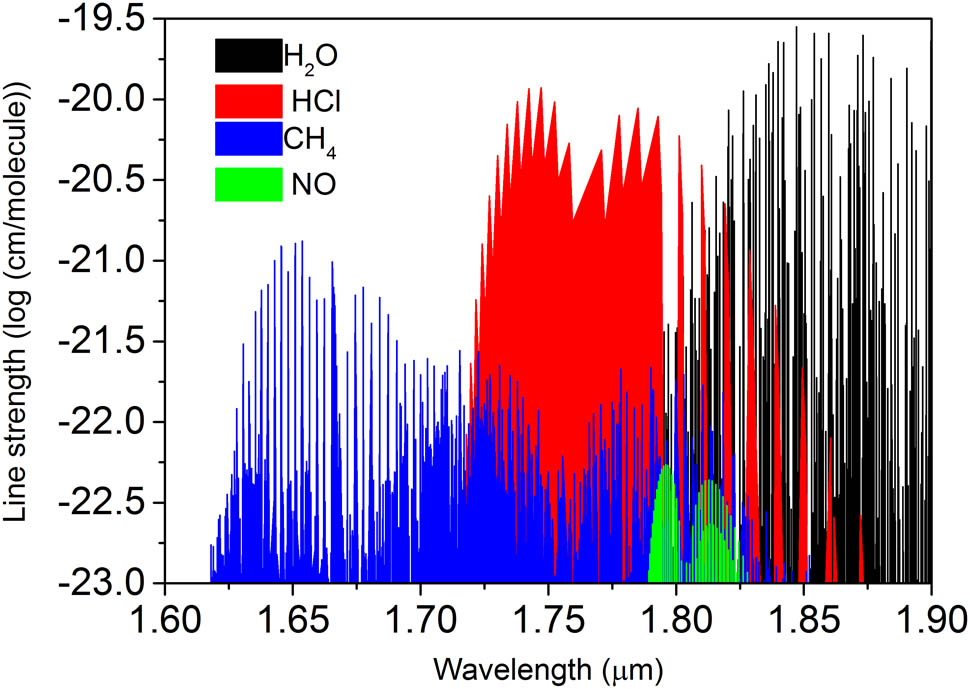
We report a 1.8 μm two-section distributed Bragg reflector laser using butt-jointed InGaAsP bulk material as the waveguide core layer. The threshold current is 17 mA and the output power is 8 mW on average. The threshold current, output power, and emitting wavelength dependences on temperature are measured. The obtained wavelength tuning range is 10 nm. This device has potential applications in simultaneous multiple-gas detection.Nowadays, tunable diode laser absorption spectroscopy (TDLAS) is a powerful tool in applications of gas detection and analysis, because of its rapid and contactless technology. The realization of a highly precise trace-gas TDLAS sensing system requires a tunable and single-mode laser source. Currently, in order to detect multiple gases simultaneously, several distributed feedback (DFB) lasers are employed[1], which makes the TDLAS system bulky and complex. In contrast, a distributed Bragg reflector (DBR) laser with single-mode operation can provide better performance due to its large tuning range, compared to DFB lasers. As the absorbing lines of the detected gases are covered in the tuning range of the DBR laser, it is convenient to detect several gases simultaneously using a single DBR laser[2,3]. At present, due to the rapid development of telecommunications, many DBR lasers in the wavelength range from 1.3 to 1.6 μm have been reported[4–8]. These lasers have mature fabrication technology and excellent performances. However, few attempts of fabricating DBR lasers locating at 1.6–1.9 μm have been reported[9]. The 1.6–1.9 μm wavelength band contains absorbing lines of various gases, such as NO, , HCl, and , as shown in Fig. 1. Therefore, in order to detect these gases simultaneously and conveniently, it is necessary to develop DBR lasers emitting at a wavelength range of 1.6–1.9 μm.

Figure 1.Absorption lines of , HCl, , and NO as a function of wavelength, in the spectral range from 1.6 to 1.9 μm. Data are taken from the HITRAN database.
Butt-joint is one of the technologies of fabricating DBR lasers. Wet chemical etching[10], reactive-ion-etching (RIE) followed by HBr-based solution,[11] and RIE followed by selective wet etching[12] are three methods reported on the fabrication of these butt-coupled optical devices. For the lasers in the spectrum range of 1.6–1.9 μm, an InGaAs quantum-well material is often employed, which is a little different from that within the 1.35–1.5 μm range with InGaAsP material. The selective undercut etch of the InGaAs quantum well has been especially studied[13]. However, there are few works about the etching process for butt-joint or optical integration of InGaAs quantum-well materials.
In this Letter, we report a two-section DBR laser diode emitting at 1.8 μm for the first time (to our knowledge). The laser was fabricated with butt-joint technology. An optimized wet etchant solution was used in the etching process. The threshold current, output optical power, and emitting wavelength were investigated as a function of temperature. A maximum wavelength tuning range of 10 nm was obtained at 25 °C. In this range, absorbing lines of four kinds of gases, as shown in Fig. 1, are covered. Therefore, we anticipate this DBR laser has potential applications in TDLAS system to detect various gases simultaneously.
Sign up for Chinese Optics Letters TOC. Get the latest issue of Chinese Optics Letters delivered right to you!Sign up now
A schematic illustration of the two-section DBR laser is shown in Fig. 2(a). The DBR laser was fabricated through three steps of metal–organic chemical vapor deposition (MOCVD) growth procedures. In the first growth step, an -InP buffer layer, a strained separate confinement heterostructure (SCH) multiquantum-well (MQW), and a 5 nm InP protect layer were grown in sequence. The strained SCH MQW consisted of four pairs of 7 nm compressively strained InGaAs (, where PL stands for photoluminescence) wells and 12 nm five tensile strained InGaAsP () barriers embedded in two undoped InGaAsP () separate confinement layers. Then a 30 μm wide and 400 μm long mask pattern corresponding to the active region was aligned along the [110] direction on the growth wafer using the photolithography process. Traditionally, a selective etchant () was used in devices with an InGaAsP quantum well for passive region etching[7], where the lower the P-content of InGaAsP in the layer, the higher the etch rate[13]. In order to avoid severe undercut at the interface of the active and passive regions, an optimized solution of () was adopted. Thus, with the protection of the mask, the SCH and MQW layers in the Bragg section were directly etched by the selective etchant, (), for 7 min, and then subjected to a chemically cleaning for 30 s using in freezing point before the regrowth. Then the second growth step for butt coupling was performed by growing a 340 nm thick undoped InGaAsP () waveguide core layer, which is matched to the InP substrate in the lattice. The PL spectra of the active region and passive waveguide region are shown in Fig. 2(b). It is shown that the bandgap wavelength of the butt-joint material is far away from the PL peak of the active region, thus the absorption loss of the passive section is sufficiently low[14]. A scanning electron microscope (SEM) image of the cross section of the butt-jointed interface between the active region and the passive waveguide region is shown in the inset of Fig. 2(a). An ideal butt-jointed shape is obtained at the interface of the regrown region and the active region. There are also no visible defects at the interface, which is necessary for a high coupling efficiency of butt-jointed devices.
Figure 2.(a) Schematic of two-section DBR laser structure. Inset, SEM image of butt-jointed interface between active region and passive waveguide; (b) PL spectra of the active region material and the passive region material. Bragg wavelength before tuning is also marked with a blue dot.
After the MQWs and waveguide layers were butt jointed on the InP substrate, a grating was formed on the waveguide core layer of the Bragg section using conventional holographic exposure and dry etching. Then, a -type InP cladding layer and a -type InGaAs contact layer were grown over the whole structure after removal of the film in the third growth step. A 3 μm wide ridge waveguide, which providing lateral optical confinement, was fabricated by removing the cladding and contact layers using conventional photolithography and wet chemical etching. A 50 μm wide isolation between the gain section and DBR section was realized by etching off the -InGaAs layer and implantation. A insulation layer, which providing current confinement, was deposited and the window was opened on the top of the ridge waveguide. Then Ti/Au was sputtered on the side for -contact and AuGeNi/Au was vaporized onto the side of the chip after the wafer was lapped to 100 μm. The chip was cleaved with a 350 μm gain section and 400 μm Bragg section. Both facets of the devices were uncoated. The chips were mounted on Cu submounts with the -side upward for continuous-wave (CW) measurements.
The optical output power characteristics versus gain current () were measured at various temperatures, as shown in Fig. 3, where the Bragg section current () is 0 mA. The output light is coupled out from the facet of the gain section and measured using a Thorlab integrating sphere and Keithley photodeiode meter. The threshold current is 15 mA at 15 °C and increases to 19.5 mA at 30 °C. The calculated characteristic temperature of the threshold current is 59 K between 15 and 30 °C, which is comparable to that of a conventional 1.55 μm laser. When the temperature increases from 15 to 30 °C the output power decreases from 9.7 to 7.8 mW. As can been seen, the output power is insensitive to the temperature variation when the gain current increases from the threshold current to about 80 mA. This is due to the material gain peak moving to the lasing wavelength and thus the increased gain counteracts partial Auger recombination as the temperature increases. Although Auger recombination is serious in lasers with long wavelength emission, we still obtain the low threshold current and comparative output power compared to previously reported 1.55 μm DBR lasers with a similar structure[7].
Figure 3.Optical output power characteristics versus gain current at various temperatures. Bragg section current is 0 mA. Inset, threshold current dependence on the temperature.
However, Fig. 3 shows that as gain current increases, there is a kink in the P–I curve. This is due to mode-hopping. We confirmed it by measuring the emitting wavelength at different gain current around the kink, as shown in Fig. 4, together with the P–I curve of the laser at 25 °C. As can be seen, there is an obvious blue shift of the wavelength around the gain current where the kink appears. This also contributes to the output power rise when the gain current is beyond the kink point. As the wavelength of the material gain peak (around 1.78 μm) is a little far from the Bragg wavelength (1.8 μm) determined by the grating, as shown in Fig. 2(b), the blue shift makes the emitting wavelength moving towards the gain peak and causes the output powers to increase faster.
Figure 4.Output power and emitting wavelength as a function of gain current.
The lasing spectra as a function of temperature are reported in Fig. 5, where is fixed to 80 mA and is 0 mA. As the temperature increases from 15 to 30 °C, the emission wavelength red shifts from 1801.78 to 1804.46 nm with the single-mode suppression ratios (SMSRs) larger than 40 dB. The wavelength tuning rate of the temperature is calculated to be about . This relatively high tuning rate of the temperature provides an effective means to extend the tuning range of the DBR laser. However, it also means a strict temperature control is required when a certain wavelength is needed.
Figure 5.Lasing spectrum as a function of temperature with fixed gain current of 80 mA.
Figure 6 shows the tuning range obtained by changing at 25 °C, where the gain current was fixed to 80 mA. As the Bragg current increases from 0 to 140 mA, the emitting wavelength is around 1800 nm and a maximum tuning range of 10 nm is obtained. It should be noted that in this tuning range there are several absorbing lines of NO, , HCl, and . The overlapped spectra of different wavelengths were measured and are shown in Fig. 7. It is shown that the lasing wavelength blue shifts as the Bragg current increases. For the first eight channels, the output power change is less than 1.1 dB when changing the Bragg current. In contrast, the output power decreases about another 1 dB when the laser emits at the last channel. This relatively large power change is mainly due to the influence of the self-heat effect. However, there is only a 0.27 nm wavelength tuning in the last channel. Except the narrow regions where mode-hopping happens, the SMRS is over 25 dB, which is enough for gas detection, in the whole tuning range.
Figure 6.Tuning range obtained by only changing at 25 °C. is fixed to 80 mA. Maximum tuning range of 10 nm is obtained.
Figure 7.Overlapped spectra of different wavelength when changing the current of the Bragg section only.
In conclusion, a two-section DBR laser emitting at a wavelength of 1.8 μm is demonstrated. The device is fabricated by butt-joint technology with an optimized etching process. The average threshold current and output power of the laser are around 17 mA and 8 mW, respectively. The laser has a maximum tuning range of 10 nm and the SMRS are all above 25 dB. Therefore, this two-section DBR laser can be a potential light source for TDLAS systems for detecting multiple gases simultaneously.
References
[1] J.-P. Besson, S. Schilt, L. Thévenaz. Spectrochim. Acta Part A, 60, 3449(2004).
[2] R. Phelan, M. Lynch, J. F. Donegan, V. Weldon. Appl. Opt., 44, 5824(2005).
[3] J. Shao, Y. Han, L. Juo, L. Wang, Y. Han, Z. Zhou, R. Kan. Appl. Opt., 52, 7462(2013).
[4] S. Murata, I. Mito, K. Kobayashi. Electron. Lett., 23, 403(1987).
[5] K. Shinoda, T. Kitatani, M. Aoki, M. Mukaikubo, K. Uchida, K. Uomi. IEEE Photon. Technol. Lett., 18, 2383(2006).
[6] S. Afzal, F. Schnabel, W. Scholz, J. P. Reithmaier, D. Gready, G. Eisenstein, P. Melanen, V. Vilokkinen, I. Montrosset, M. Vallone. IEEE Photon. Technol. Lett., 23, 411(2011).
[7] L. Han, S. Liang, C. Zhang, L. Yu, L. Zhao, H. Zhu, B. Wang, C. Ji, W. Wang. Chin. Opt. Lett., 12, 091402(2014).
[8] Q. Kan, Y. Ding, L. Zhao, H. Zhu, F. Zhou, L. Wang, B. Wang, W. Wang. Chin. Opt. Lett., 3, 455(2005).
[9] B. Niu, H. Yu, L. Yu, D. Zhou, L. Zhao, J. Pan, W. Wang. Proc. SPIE, 8555, 85550Z(2012).
[10] T. Brenner, E. Gini, H. Melchior. IEEE Photon. Technol. Lett., 5, 212(1993).
[11] J. Ahn, K. R. Oh, C. Park, S. G. Han, H. G. Kim, B. Lee, D. Kim, C. Park. Semicond. Sci. Technol., 13, 1205(1998).
[12] S. H. Oh, C. W. Lee, J. M. Lee, K. S. Kim, H. Ko, S. Park, M. H. Park. IEEE Photon. Technol. Lett., 15, 1339(2003).
[13] D. Pasquariello, E. S. Bjorlin, D. Lasaosa, Y. J. Chiu, J. Piprek, J. E. Bowers. J. Lightwave Technol., 24, 1470(2006).
[14] L. Yu, H. Wang, D. Lu, S. Liang, C. Zhang, B. Pan, L. Zhang, L. Zhao. IEEE Photon. J., 6, 1501308(2014).