1Department of Communication Science and Engineering, Key Laboratory for Information Science of Electromagnetic Waves (MoE), Fudan University, Shanghai 200433, China
2National Institute of LED on Silicon Substrate, Nanchang University, Nanchang 330096, China
Visible light communication based on light-emitting diodes (LEDs) has become a promising candidate by providing high data rates, low latency, and secure communication for underwater environments. In this paper, a self-designed common-anode GaN-based five-primary-color LED (RGBYC LED) on a Si substrate is proposed and fabricated. The design of a common anode is used to mitigate the saturation effect for a low-frequency component. Additionally, compared with commercially available LEDs that suffer from nonlinearity distortion, applying the designed LED can provide much better and broader linearity according to the measurement results. Therefore, the modulation depth and system performance can be further improved to implement a high-speed underwater visible light communication (UVLC) system. There is no nonlinearity compensation algorithm applied due to the good linearity of the proposed LED; thus, the offline digital signal processing is simplified. We experimentally demonstrate 14.81 Gbit/s 64 quadrature amplitude modulation (QAM)-discrete multitone (DMT) and 15.17 Gbit/s bit-loading-DMT transmissions through a 1.2-m-long underwater channel based on the proposed RGBYC LED with an intrasymbol frequency-domain averaging channel estimation and zero-forcing equalization. As far as we know, this is the highest data rate for an LED-based UVLC system.
1. INTRODUCTION
With more and more human underwater activities, the demand for efficient underwater communication is increasing. Nowadays, the most widely applied method for underwater wireless communication is acoustic technology. However, it is still limited by low bandwidth, high transmission attenuation, high latency, the multipath effect, and Doppler spread. Applying radio frequency (RF) communication in an underwater environment is restricted by the high attenuation of RF waves in seawater. Another optional way is utilizing fiber optic technology to implement long-range and high-bandwidth underwater communication. But, it is not adequate for remotely operated underwater vehicles and autonomous underwater vehicles because of the requirement of a physical cable connection between transmitters and receivers. Thus, militaries, industries, and research institutions have shown great interest in underwater wireless optical communication (UWOC), which is considered as an alternative or complement to the existing underwater communication technologies mentioned above [1–3]. In recent years, visible light communication (VLC) has drawn increasing attention due to several advantages such as high security, low cost, immunity to electromagnetic interference, and that it is license-free [4–6]. It is a promising candidate for next-generation UWOC considering the relatively low attenuation window of seawater in the blue–green portion of the electromagnetic spectrum, which is around the visible light region. Underwater visible light communication (UVLC) is expected to play an important role by providing high data rates, low latency, and secure communication within a short range [1,2]. Laser diodes (LDs) and light-emitting diodes (LEDs) are two commonly used transmitters for UVLC systems. LDs can support longer distance transmission in point-to-point scenarios because of higher power density, but require accurate alignment between transmitters and receivers. 5.2 and 10.8 Gbit/s 16 quadrature amplitude modulation (QAM)-orthogonal frequency division multiplexing (OFDM) transmissions over 10.2 m based on LDs are implemented in Refs. [7,8]. Compared with LDs, LEDs have much wider divergence, which can be applied for shorter distance links in both point-to-point and point-to-multipoint scenarios. Applying LEDs will survive the sparkle effect because of the noncoherent nature. Besides, LEDs are much cheaper than LDs and can be integrated into large-scale arrays to achieve high illumination power of hundreds of watts.
In the past two decades, GaN-based LEDs have been intensively investigated and developed. Sapphire is the most commonly used substrate for commercially available GaN-based LEDs [9]. The SiC substrate is also applied for GaN-based LEDs for only 3.5% lattice mismatch with GaN and good electrical conductivity [10]. The Si substrate is more promising for GaN-based LEDs compared with sapphire and SiC due to the merits of lower cost, larger size, higher crystal quality, and better electrical conductivity [11]. The GaN film grown on a Si substrate can be lifted off easily utilizing the chemical wet-etching technique, while a laser is required to separate the GaN film from SiC and sapphire substrates, which might damage the film and thus influence the performance of LED devices [12]. In addition, only lateral-structure LEDs can be fabricated with GaN film grown on the sapphire substrate if the GaN film is not lifted off from the substrate due to the insulating nature of sapphire. This structure suffers from serious current crowding and current droop when operated at a high-driving current density, and this may result in the rising of junction temperature. But, the heat cannot be conducted effectively due to the poor heat conductivity of the sapphire substrate, which may damage LED performance dramatically. Fortunately, a Si substrate has high heat conductivity, which is an excellent option to solve this problem. Our recent achievements utilizing LEDs based on a Si substrate are summarized in Table 1. These results clearly validate the feasibility of applying LEDs based on a Si substrate in both UVLC and VLC systems. However, these LEDs are all designed as a common cathode, which still suffers from the saturation effect for a low-frequency component. An 11.95 Gb/s VLC transmission based on a violet micro-LED is reported in Ref. [23], but this kind of LED has output power with a magnitude of a milliwatt. That is to say, it can only be used in a dark environment and for a short transmission distance.
LED Type
Modulation Format
Data Rate
Distance
Data Source
RGBYC WDM
64QAM-DMT
10.72 Gbit/s
1 m free space
OFC 2018 [13]
RGBYC green
64QAM-DMT
1.725 Gbit/s
1.2 m underwater
ICEVLC 2018 [14]
RGBYC blue
PAM8
1.5 Gbit/s
1.2 m underwater
OE 2018 [15]
RGBYC blue
PAM7
1.312 Gbit/s
1.2 m underwater
IMCO 2018 [16]
RGBYC blue
GCS 8QAM
1.62 Gbit/s
1.2 m underwater
ACP 2018 [17]
RGBYC blue
CAP64, OFDM, and DFT-S OFDM 64QAM
3 Gbit/s
1.2 m free space and underwater
COL 2018 [18]
RGBYC green
64QAM-DMT
2.175 Gbit/s
1.2 m underwater
OC 2018 [19]
RGBYC green
MISO PAM7
918.75 Mbit/s
2.1 m free space and underwater
JLT 2018 [20]
RGBYC blue
SIMO 16/32QAM-DMT
1.8 Gbit/s
1.2 m underwater
AO 2019 [21]
RGBYC blue
SGS 32/128QAM
2.534 Gbit/s
1.2 m underwater
OC 2019 [22]
Table 1. Recent Achievements Applying LEDs Based on a Si Substrate
In this paper, a self-designed GaN-based common-anode red–green–blue–yellow–cyan LED (RGBYC LED) on a Si substrate is proposed and fabricated, which can reduce the low-frequency component to mitigate the saturation effect. Compared with the violet micro-LED, it has larger output power with a magnitude of a watt and higher linearity with a higher driving current. Additionally, it can be used in an environment with background light. It is noted that GaN-based LEDs are more efficient in the short wavelength range and the efficiency decreases dramatically when the wavelength exceeds 530 nm. Therefore, the red LED chip is made by an AlGaInP material system with an AsGa substrate to maintain high efficiency when the wavelength is greater than 590 nm. But for blue, green, yellow, and cyan chips, they are all based on a GaN material system with a Si substrate. The RGBYC LED is successfully applied in a UVLC system through experiments. 14.81 Gbit/s 64 QAM-discrete multitone (64QAM-DMT) and 15.17 Gbit/s bit-loading-DMT transmissions through a 1.2-m-long underwater channel based on this designed LED with an intrasymbol frequency-domain averaging (ISFA) channel estimation and zero-forcing equalization are implemented. As far as we know, it is the highest data rate for an LED-based UVLC system.
Sign up for Photonics Research TOC. Get the latest issue of Photonics Research delivered right to you!Sign up now
2. DESIGN AND FABRICATION OF THE LED CHIP
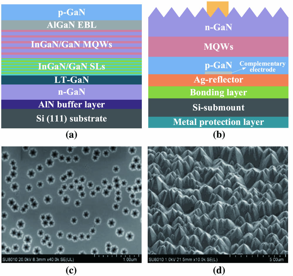
There is about 17% lattice mismatch between GaN () and Si (). As we all know, large lattice mismatch leads to high dislocation density in epitaxial materials. In addition, the most severe problem is around 46% thermal expansion mismatch between GaN and Si. The thermal expansion coefficient of GaN is and for Si [24]. The upshot is that bending or cracking of the epitaxial wafer occurs massively when GaN films are subjected to great stress during cooling. Therefore, the fabrication of a patterned Si(111) substrate is one of the key technologies to generate high-quality crack-free thin GaN film growing in a Si substrate selection. Usually, the size of unit graphics depends on the size of the chip obtained in the end. A Si substrate graphics unit can be continuously adjusted from to [25]. The size of acquired chips meets all aspects of existing GaN-based LED applications. In this experiment, the epitaxial layers are grown on a patterned Si(111) substrate by a homemade metal organic chemical vapor deposition (MOCVD) system. Trimethyl-gallium (TMGa), trimethyl-indium (TMIn), trimethyl-aluminum (TMAl), and ammonia (NH3) are used as the source materials of Ga, In, Al, and N, respectively. Silane (SiH4) and bis-cyclopentadienyl magnesium (Cp2Mg) are used as the -type and -type doping sources. As shown in Fig. 1(a), the epitaxial structure begins with a 110 nm high-temperature AlN (HT-AlN) buffer layer to avoid the reaction between NH3 and the silicon substrate. Then a 2.8 μm -type GaN layer with Si doping of 5 × 1018 cm−3 is grown. Subsequently, a 10 nm low-temperature GaN (LT-GaN) layer is deposited and followed by a superlattice (SL) interlayer with 32-period of In0.05Ga0.95N/GaN (5/2 nm) grown. V-pits can easily initialize at the sites of dislocations within the SLs. The active region includes 7–9 periods of InGaN/GaN milti-quantum wells (MQWs). Firstly, a 0.5 nm GaN cap layer is grown with the purpose of repairing the damaged surface during the changing of temperature. Then the InxGa1–xN (x = 0.15–0.3) well is grown with an optimum thickness of 2.5 nm and covered by a 2 nm GaN protective cap before the temperature is up to grow a 13 nm GaN barrier. The barriers are slightly doped with 5 × 1017 cm−3 Si to reduce operating voltage. Finally, a 10 nm p-Al0.2Ga0.8N electron blocking layer (EBL) doped with 1 × 1019 cm−3 Mg and a heavily Mg-doped (2 × 1019 cm−3) p-type GaN layer (130 nm) are grown. The inverted hexagonal pits called V-shaped pits diffuse widely in the GaN epitaxial film. As a typical feature of GaN-based LEDs, V-shaped pits play an important role in preventing nonradiative recombination of carriers in threading dislocation. Accordingly, the size and density of V-shaped pits are regulated via different growth parameters to improve luminous efficiency when the GaN film is grown [26,27]. Figure 1(c) is the scanning electron microscope (SEM) image of V-shaped pits on the surface of MQWs.
Figure 1.(a) Schematic of GaN-based LED epitaxial structure on the Si substrate, (b) vertical structure of the LED chip on the Si substrate, (c) SEM image of V-shaped pits on the surface of MQWs, and (d) SEM image of texture surface.
After epitaxial growth, the LED epitaxial wafer is fabricated into a vertical structure chip using the standard LED fabrication process. First, a layer of metal Ag is deposited on the clean epitaxial wafer by an electron beam evaporator, which has high reflectivity and good ohmic contact with p-GaN. Then, the bonding layer is deposited on one side of a prepared Si-submount with excellent electrical conductivity and thermal conductivity (-type doping, with less than resistivity and 200 μm thickness), and the metal protection layer is deposited on the other side of the Si-submount. Next, the wafer is bonded on the Si-submount, and then the Si substrate is removed using the mixed solution of HF, , and . Finally, the n-GaN surface is roughened by submerging it into 85°C and 20% mass concentration KOH solution, and then the n-electrode is processed on the rough n-GaN [28,29]. The schematic of the LED chip’s vertical structure on the Si substrate is shown in Fig. 1(b). Applying a vertical structure has many advantages, such as single-side luminescence, better light-emitting uniformity, and better direction. In order to improve light extraction efficiency, the surfaces of vertical-structure LED dies are also textured with hemispherical and pyramidal patterns, as shown in Fig. 1(d). A specially designed Ag reflector is used to improve single-side luminescence. Current crowding is one of the most serious problems when the LED chip is operated at high driving current. Therefore, the high resistance complementary electrode is designed to alleviate current crowding, and also increases single-side luminescence area and uniformity.
The bracket used in this design has 12 pins, as shown in Fig. 2(a). The LED dies are directly attached to the heat sink of the bracket by conductive silver paste. High thermal conductivity and high adhesion CT285 silver glue are used to attach the LED chip to the heat sink to achieve the mechanical connection between the chip and the bracket. It has volume resistivity, 25 W/mK thermal conductivity, and 40 N die shear strength at 25°C. First, the silver glue is coated in the corresponding position of each LED chip and affixed to the chip. The silver colloid is then sintered in 180°C curing for 2 h. Subsequently, the gold wire is used to achieve the electrical connection between the chip and the bracket by a golden wire ball ultrasonic welding machine. The diameter of the gold wire is 20 μm. A lens is assembled on the LED package bracket, and high-transmittance and high-refractive-index epoxy silicone (Dow Corning OE-6662, refractive index 1.53, transmittance 90%) is injected into the gap between the lens and the LED package module. Finally, the entire packaged module is heated by the oven at 150°C and kept for an hour of silicone curing. The light distribution curve is shown in Fig. 2(e). The bottom of the vertical structure chip on the Si substrate is the anode electrode, and the top is the cathode electrode; thus, the positive poles of all LED dies are the common terminal due to the conductivity of the heat sink. The anode and cathode of the chip are connected to the pins of the bracket through electric connection lines. The RGBYC (red, 623 nm; green, 521 nm; blue, 457 nm; yellow, 562 nm; cyan, 486 nm) vertical structure LED chips including one red chip, one green chip, one blue chip, one cyan chip, and two yellow chips are packaged in one LED lamp. Note that there are two yellow chips employed to increase the yellow light output power because yellow LEDs still suffer from limited quantum efficiency. After nearly 10 years of exploration, our team first made a breakthrough in the technologies of material growth and thin-film chip manufacturing for high-efficiency GaN-based yellow LED on a Si substrate in the world. We achieved 24.3% wall plug efficiency of yellow LED (the dominant wavelength is 565 nm under ) on a Si substrate, which is the reported highest value to the best of our knowledge [30]. The luminous efficiency of red, blue, cyan, green, and yellow LED chips is about 80–90 lm/W, 25–30 lm/W, 40–50 lm/W, 180–200 lm/W, and 130–150 lm/W at , respectively. Due to the identity of the two yellow chips, the results for only one yellow chip are provided to avoid duplication. The schematic of the chips’ layout and bonding is shown in Fig. 2(b). Different from our previous design of a common cathode, this package layout is designed as a common anode, which can reduce low-frequency response to mitigate the saturation effect for the low-frequency component. The SEM and optical microscope images of the packaged device are shown in Figs. 2(c) and 2(d), respectively.
Figure 2.Schematic of (a) bracket structure and (b) chip layout; (c) SEM and (d) optical microscope images of the packaged device; and (e) the light distribution curve of the LED lamp (the unit of the numbers on the circle is degree).
Relative light output power versus current, relative wall plug efficiency versus current density, and relative luminous efficiency versus current density for the five color chips are shown in Fig. 3. It is well known that the nonlinearity characteristics of commercially available LEDs are one of the main obstacles for current high-speed VLC systems, which may cause amplitude distortion and signal clipping [31,32]. According to Fig. 3(a), there is good linearity for different color chips of the designed RGBYC LED on the Si substrate. With such a broad linear range, utilizing the fabricated LED can further improve modulation depth and signal-to-noise ratio (SNR) for high-speed VLC systems. Figure 4 shows the measured electroluminescence (EL) spectra with different injection current for the five chips. Figure 5 shows the corresponding Commission Internationale de l’Eclairage (CIE) diagrams of correlated color temperature (CCT) variation versus driving current for red, green, blue, yellow, and cyan LED chips. CCT changes from 44,380 K to 15,512 K, 100,000 K to 28,700 K, 10,328 K to 100,000 K, and 21,466 K to 28,760 K for red, green, blue, and cyan chips, respectively, with the driving current changing from 80 to 200 mA. As for the yellow chip, CCT changes from 100,000 K to 26,360 K with the driving current changing from 120 to 200 mA. The yellow chip is restricted by limited quantum efficiency; thus, it requires higher driving current.
Figure 3.(a) Relative light output power versus current, (b) relative wall plug efficiency versus current density, and (c) relative luminous efficiency versus current density.
The block diagram of DMT modulation is shown in Fig. 6. As a typical multicarrier modulation technique, DMT modulation is a variant of OFDM modulation, which utilizes Hermitian symmetry to generate a real-valued signal for VLC transmission. After serial-to-parallel conversion, a portion of subcarriers at both ends are set as zeros, which is called zero padding. The generated DMT signals are defined as where N represents inverse discrete Fourier transform (IDFT) size, and it is even; N/2 is the subcarrier number; is the M-QAM symbols on the th subcarrier; and satisfies where * represents the conjugation operation.
At the receiver side, demodulation of the DMT signal is implemented by N-point IDFT, which can be written as where is the received M-QAM symbols on the th subcarrier. A training sequence is inserted in the transmitted signal to implement channel estimation. The estimated channel can be expressed as where is the estimated channel frequency response and is the received training sequence.
The obtained channel frequency response is critical to the following zero-forcing equalization. An ISFA scheme is applied to improve the channel estimation accuracy with noise, and thus the frequency response for each subcarrier is averaged by itself and its multiple adjacent subcarriers. Typically, the averaging is performed over a subcarrier and its right and/or left neighbor subcarriers or totally up to adjacent subcarriers [33]. The smoothed channel frequency response for the th subcarrier can be written as where and represent the maximum and minimum effective modulated subcarrier indexes, respectively. Based on , the transmitted signal can be recovered using zero-forcing equalization as Nowadays, forward error correction (FEC) is not included in many optical transmission simulations and experiments. Thus, thresholds are widely utilized to decide if the bit error rate (BER) is in the target range of to . Pre-FEC BER is the most commonly used threshold. However, in recent years, generalized mutual information (GMI) is discussed and applied as an alternative way to predict post-FEC BER with higher accuracy [34–36]. According to Ref. [34], the probability distribution of a received symbol in a memoryless additive white Gaussian noise (AWGN) channel can be expressed as where is the noise variance and is the transmitted symbol. The maximum number of bits that can be carried by a symbol based on M-QAM constellation is defined as According to Ref. [34], GMI quantifying the maximum number of information bits per symbol can be estimated by where represents the M-QAM symbol set, is the number of transmitted symbols, is the th bit of the th transmitted symbol, and represents the M-QAM symbol set whose th bit value is . Once GMI is obtained, the achievable information rate (AIR) is given by where BW is the signal bandwidth.
Bit-loading-DMT can be applied to further increase AIR. A binary phase shift keying (BPSK)-DMT signal is transmitted at first to estimate the SNR distribution for each subcarrier. More bits are allocated to subcarriers with higher SNR. From Ref. [37], the SNR for each subcarrier is calculated based on error vector magnitude (EVM) as where is the normalized th received symbol, is the th symbol’s respective ideal normalized constellation point, and represents the number of unique symbols in the constellation. From Ref. [37], BER can be represented as where is the level number in each dimension in M-QAM modulation system, and is the Gaussian coerror function defined as By utilizing the relationship between BER and SNR, the maximum allocated bit number for each subcarrier can be estimated with a BER threshold of . And then, the bit-loading-DMT signal is generated and transmitted based on the estimated bit-allocation result. The GMI and AIR for bit-loading-DMT transmission are defined as where is the number of unique estimated bit numbers for all the subcarriers, is the probabilistic of the bit number of , and is the GMI value with bit number modulation.
B. Experimental Setup
Figure 6 shows the experimental setup of the 64QAM-DMT and bit-loading-DMT transmission through a 1.2-m-long underwater channel utilizing the self-designed RGBYC LED. At the transmitter side, the digital 64QAM-DMT/bit-loading-DMT signal is generated by an offline MATLAB program. The generated signal is then loaded into an arbitrary waveform generator (AWG, Tektronix AWG710). After that, a hardware pre-equalization circuit is applied to compensate for the channel attenuation of high-frequency components [38]. The equalized signal is amplified by an electrical amplifier (EA, Mini-Circuits, 25 dB gain) and then coupled with direct current by bias tee (Mini-Circuit ZFBT-4R2GW-FT+). The RGBYC LED is employed as the transmitter and driven by the direct current. To achieve wavelength division multiplexing (WDM), signals from five channels are modulated to the five chips of the RGBYC LED simultaneously. It is noted that only one yellow chip of the RGBYC LED is used, and thus in total, there are five channels of signals. At this time, the signals are converted to optical signals. In order to emit parallel light into the water, a lens (70 mm diameter and 100 mm focus length) is placed after the RGBYC LED. A 1.2 m water tank is applied to achieve underwater transmission. After 1.2 m UVLC transmission, another lens (70 mm diameter and 100 mm focus length) is used to focus the receiving light. At the receiver side, a differential receiver including a commercial PIN (Hamamatsu 10784), a transimpedance amplifier (TIA), and a differential circuit is used to detect the received signal and implement photoelectric conversion. At last, the signals are sampled by a digital sampling oscilloscope (OSC, Agilent DSO54855A) with 2 GSa/s sampling rate.
For the offline 64QAM-DMT signal-generation process, the original binary bit stream is first mapped into 64QAM symbols, and zeros are inserted into the signal. Exactly 256 subcarriers are used to load the QAM symbols. After that, the signal is combined with its conjugation and upsampled by a factor of 4. A real-valued signal is generated after 512-point IFFT. A cyclic prefix (CP) with eight samples is employed to mitigate intersymbol interference (ISI). Training symbols are used for channel estimation. At the receiver side, ISFA channel estimation and zero-forcing postequalization are applied. Due to the good linearity of the designed LED, there is no nonlinear compensation algorithm employed to mitigate the nonlinear effect of the RGBYC LED. After 64QAM demapping, the original bit sequence is recovered. To further increase the system AIR, bit-loading-DMT is also applied in the experimental demonstration. The major procedures for bit-loading-DMT signal generation and processing are the same as 64QAM-DMT except that the BPSK-DMT signal is transmitted at first to test the SNR of each subcarrier. The bit numbers allocated for each subcarrier are estimated according to SNR distribution. Then, M-QAM mapping for each subcarrier is achieved by the corresponding allocated bit numbers.
4. EXPERIMENTAL RESULTS AND DISCUSSION
A. 64QAM-DMT
The forward transmission gains without and with a pre-equalizer are shown in Fig. 7. It is clear that the bandwidth of the UVLC system can be improved dramatically by applying the hardware pre-equalizer. Then, the transmission points with the optimal peak-to-peak voltage (Vpp) and the optimal driving current of the LED chips are tested, as shown in Fig. 8. The operation range is circled by a black line of FEC threshold. According to the measurement results, the red, green, blue, cyan, and yellow LED chips are operated at the optimal transmission points with 0.9 V Vpp and 100 mA current, 1.2 V Vpp and 180 mA current, 1.2 V Vpp and 160 mA current, 1.8 V Vpp and 180 mA current, and 1 V Vpp and 180 mA current, respectively. The measured color-rendering index (CRI) is 85.4, and the CCT is 32,800 K with all five chips working at the corresponding optimal transmission point. The white light point synthesized by red, green, blue, yellow, and cyan chips under a driving current of 140 mA, 40 mA, 60 mA, 80 mA, and 200 mA, respectively, meets the need for most indoor lighting. This point, which features CCT 5880K and CRI 81.8, is referenced as the good illumination point in the following content. The CIE diagram showing chromaticity coordinates of the RGBYC LED operated at the optimal transmission point and the good illumination point is presented in Fig. 9(a). Considering the current differences between the good illumination point and the optimal transmission point, there is a trade-off between illumination and transmission performance. The optical spectra at the optimal transmission and the good illumination points are shown in Figs. 9(b) and 9(c). The blue light portion has the highest power intensity, and the green light portion’s power intensity is relatively higher than the other three kinds of light, which coincides with the fact that VLC has a relatively low attenuation window of seawater in the blue–green portion of the electromagnetic spectrum.
Figure 7.Measured forward transmission gains (a) without pre-equalizer and (b) with pre-equalizer.
Figure 9.(a) CIE diagram showing the chromaticity coordinates of RGBYC LED operated at (i) the optimal transmission working point and (ii) the good illumination point; optical spectra at (b) the optimal transmission working point and (c) the good illumination point; (d) AIR versus bandwidth; insets, the highest data rate points for (iii) red chip, (iv) green chip, (v) blue chip, (vi) yellow chip, and (vii) cyan chip.
The AIR of the designed RGBYC LED versus bandwidth utilizing GMI is measured and shown in Fig. 9(d). Applying the red chip can achieve 3.0119 Gbit/s with 525 MHz, the green chip can achieve 3.0703 Gbit/s with 537.5 MHz, the blue chip can achieve 3.0436 Gbit/s with 525 MHz, the yellow chip can achieve 2.6254 Gbit/s with 525 MHz, and the cyan chip can achieve 3.0581 Gbit/s with 525 MHz. Thus, a total AIR of 14.8093 Gbit/s based on one RGBYC LED applying WDM is successfully achieved. The measured electrical spectra of the five color chips are shown in Fig. 10. Applying a hardware pre-equalizer can significantly flatten the electrical spectra, and the data rate cannot be further increased even with higher bandwidth due to lower BER.
Figure 10.Measured electrical spectra for red chip using 600 MHz bandwidth (a) with and (b) without pre-equalizer, for (c) red chip, (d) green chip, (e) blue chip, (f) yellow chip, and (g) cyan chip with pre-equalizer and respective optimum bandwidth applying 64QAM-DMT modulation; electrical spectra for (h) red chip, (i) green chip, (j) blue chip, (k) yellow chip, and (l) cyan chip with pre-equalizer applying bit-loading-DMT modulation.
Bit-loading-DMT transmission is further implemented to explore the highest system AIR. Vpp and the driving current are set at their optimum values. Then, the highest AIR is measured by changing the bandwidth, as shown in Fig. 11. Thus, the highest data rate is 3.0393 Gbit/s with 600 MHz bandwidth, 3.1014 Gbit/s with 600 MHz bandwidth, 3.1295 Gbit/s with 575 MHz bandwidth, 2.7885 Gbit/s with 600 MHz, and 3.1131 Gbit/s with 602.5 MHz bandwidth for red, green, blue, yellow, and cyan chips respectively. The bit-loading schemes for different subcarriers implementing the highest AIR are shown in Fig. 12. Note the average allocated bit for the yellow chip is lower than for the others due to lower output power. The measured electrical spectra applying the pre-equalizer and their own optimum bandwidth for the five-color chips are shown in Figs. 10(h)–10(l), respectively. Compared with 64QAM-DMT modulation, applying bit-loading-DMT modulation can further increase system AIR. Therefore, a total AIR of 15.1718 Gbit/s is implemented based on this system. As far as we know, this is the highest data rate for an LED-based UVLC system.
Figure 11.AIR versus bandwidth; insets, the constellation diagrams at point (i).
In this paper, a self-designed common-anode GaN-based RGBYC LED on a Si substrate is proposed and fabricated. Compared with sapphire and SiC substrates, the Si substrate is preferred for GaN-based LEDs because of the advantages of lower cost, larger size, higher crystal quality, and better electrical conductivity. The common anode is designed to mitigate the saturation effect for the low-frequency component. A good linearity in a broad range of the proposed LED is found according to the measurement. Due to the good linearity of the designed LED, it can be used to achieve a high-speed VLC system in an underwater environment. Besides, there is no nonlinear compensation algorithm employed to mitigate the nonlinear effect, which simplifies the offline digital signal processing. There is a trade-off between the good illumination point and the optimal transmission point. When being operated at the optimal transmission point, the measured CRI is 85.4, and the CCT is 32,800 K. The red, green, blue, yellow, and cyan LED chips are operated at the optimal transmission point with 100 mA current, 180 mA current, 160 mA current, 180 mA current, and 180 mA current, respectively. While for the good illumination point, the CRI is 81.8, and the CCT is 5880 K. And, the applied driving current is 140 mA, 40 mA, 60 mA, 80 mA, and 200 mA for red, green, blue, yellow, and cyan chips, respectively. 14.81 Gbit/s 64QAM-DMT and 15.17 Gbit/s bit-loading-DMT transmissions are experimentally demonstrated through a 1.2-m-long UVLC channel. To the best of our knowledge, this is the highest implemented data rate in an LED-based UVLC system. Note that the designed LED still has good linearity with a driving current higher than 200 mA, and the implemented experimental system is now restricted by the driving circuit and heat dissipation. Thus, the transmission data rate can be further increased if a better driving circuit and better heat dissipation are implemented in the future.
[2] G. Cossu, R. Corsini, A. M. Khalid, S. Balestrino, A. Coppelli, A. Caiti, E. Ciaramella. Experimental demonstration of high speed underwater visible light communications. 2nd International Workshop on Optical Wireless Communications (IWOW)(2013).
[8] H. Y. Wang, Y. F. Huang, W. C. Wang, C. T. Tsai, C. H. Cheng, Y. C. Chi, G. R. Lin. Seawater communication with blue laser carried 16-QAM OFDM at 3.7 GBaud. IEEE Optical Fiber Communication Conference, Tu2I.1(2018).
[9] S. J. Pearton. GaN and Related Materials II, 7(2000).
[13] X. Zhu, F. Wang, M. Shi, N. Chi, J. Liu, F. Jiang. 10.72 Gb/s visible light communication system based on single packaged RGBYC LED utilizing QAM-DMT modulation with hardware pre-equalization. IEEE Optical Fiber Communication Conference, M3K.3(2018).
[14] Y. Zhao, C. Wang, F. Wang, Y. Liu, X. Zhu, J. Liu, F. Jiang, N. Chi. 1.725 Gb/s underwater visible light communication system based on a silicon substrate green LED and equal gain combination receiver. International Conference and Exhibition on Visible Light Communications, ICEVLC(2018).
[16] Y. Zhao, M. Shi, N. Chi. Application of multilayer perceptron in underwater visible light communication system. 8th International Multidisciplinary Conference on Optofluidics, IMCO(2018).
[17] P. Zou, Y. Liu, F. Wang, N. Chi. Mitigating nonlinearity characteristics of gray-coding square 8QAM in underwater VLC system. IEEE Asia Communications and Photonics Conference ACP(2018).
[34] J. Cho, L. Schmalen, P. J. Winzer. Normalized generalized mutual information as a forward error correction threshold for probabilistically shaped QAM. European Conference on Optical Communication (ECOC), 1-3(2017).
[37] R. A. Shafik, M. S. Rahman, A. R. Islam. On the extended relationships among EVM, BER and SNR as performance metrics. International Conference on ICECE, 408-411(2006).
[38] X. Huang, J. Shi, J. Li, Y. Wang, Y. Wang, N. Chi. 750 Mbit/s visible light communications employing 64QAM-OFDM based on amplitude equalization circuit. IEEE Optical Fiber Communication Conference, Tu2G.1(2015).