Abstract
A horizontal ridge waveguide emitter on a silicon (100) substrate with a multi-quantum-well (MQW) active layer was fabricated by molecular beam epitaxy. The device structure was designed to reduce light absorption of metal electrodes and improve injection efficiency. Electroluminescence (EL) at a wavelength of 2160 nm was observed at room temperature. Theoretical calculations indicate that the emission peak corresponds well to the direct bandgap transition (). The light output power was about 2.0 μW with an injection current density of . These results show that the horizontal GeSn/Ge MQW ridge waveguide emitters have great prospects for group-IV light sources.1. INTRODUCTION
In order to promote the development of integrated photonics, tremendous efforts have been made to broaden the reach of current silicon (Si)-based technology over the past few decades [1–3]. Thanks to the compatibility of full group-IV materials with complementary metal oxide semiconductor (CMOS) technologies, monolithic integration of group-IV materials and devices has attracted great interest [4]. Despite the development of many devices including waveguides, high-speed modulators, and detectors [5–8], an efficient light source monolithically integrated on Si remains a challenge due to the indirect bandgap nature of Si and germanium (Ge) [9]. One solution that has received renewed interest is the incorporation of the group-IV element tin (α−Sn) into a Ge lattice. Researchers have found that alloys can transform into a fundamental direct bandgap material with Sn content greater than about 8% [10–13]. Some LEDs based on GeSn bulk materials have been reported [14,15], and even some optically pumped GeSn-based lasers on Si have been demonstrated at low temperatures [16,17]. It is generally known that multi-quantum-well (MQW) structures can be used for LEDs or lasers to improve luminescence performance, and some group-IV MQW structure emitters have also been reported [18,19]. Unfortunately, most group-IV light-emitting devices are vertical structures. There is no suitable cover layer, and the problem of optical loss by the metal electrode cannot be avoided, which seriously reduces the emission efficiency [20]. In addition, to meet the requirements for monolithic integration in Si-based photonics, planar waveguide-type devices are highly desirable. In order to solve the problem of light absorption by metal contacts and considering that the waveguide is an important structure supporting light propagation and lasing, the horizontal ridge waveguide emitters were designed.
In this work, we present the epitaxial growth and structure of high-Sn-content MQWs on Si (100) substrates. In addition, the ridge waveguide LEDs with a horizontal injection structure were fabricated using a standard CMOS compatible process. The electro-optical characterization of GeSn/Ge MQW LEDs was studied. Electroluminescence (EL) from MQWs was observed at room temperature. Also, light output power with different current injection was further investigated. Based on the EL data and temperature-dependent photoluminescence (PL) spectra, the band structure of this device was discussed. Theoretical calculations by effective mass and the six-band method reveal that the band alignment can confine carriers effectively at low temperatures, and the EL is dominated by direct bandgap transition ().
2. MATERIAL GROWTH AND CHARACTERIZATION
The MQW samples were grown on Si (100) substrates with resistivity greater than by solid source molecular beam epitaxy (MBE). The complete layer sequence of nominally designed MQW structures includes: (i) a 500 nm thick Ge-buffer layer grown by a two-step growth process, in which a 70 nm thick low temperature Ge (LT-Ge) buffer layer was grown at 300°C, followed by a 430 nm thick high temperature Ge (HT-Ge) grown at 600°C; (ii) five period quantum wells grown at 190°C, well layers with a thickness of 10 nm separated by 20 nm Ge barrier layers; and (iii) a 150 nm thick Ge-cap layer deposited on the MQWs at the same temperature to avoid segregation of Sn atoms in the GeSn layer. In order to decrease the lattice mismatch dislocations, before growing the MQW structure, in situ cyclic annealing from 800°C to 600°C for five times was performed, and the duration of each cycle of annealing was 5 minutes.
Sign up for Photonics Research TOC. Get the latest issue of Photonics Research delivered right to you!Sign up now
The cross-sectional transmission electron microscopy (TEM) of the MQW heterostructure is shown in Fig. 1(a). A high crystalline quality interface is evident between the GeSn and Ge-buffer layer, and the defects in the Ge-buffer layer are limited in the LT-Ge layer. In addition, smooth and abrupt interfaces between GeSn well layers and Ge barrier layers are observed, which play an important role in the highly-effective quantum confinement effect. The inset below in Fig. 1(a) is a selected electron diffraction of the well layer, which evidences the single-crystalline nature of this layer. The inset above in Fig. 1(a) shows the energy-dispersive X-ray spectroscopy (EDX) linear scanning of elemental contents. It can be seen that the composition of Sn in the GeSn well layer is about . The high-resolution TEM image in Fig. 1(b) further reveals that the MQW interface is clear, and the thickness of the well layer is about , indicating that the thickness is well-controlled during growth. In order to verify the concentration of Sn in the GeSn well layer and obtain the strain to calculate the band diagram, the X-ray diffraction reciprocal space mapping (XRD-RSM) around the asymmetric () reflection was obtained, as shown in Fig. 1(c). It reveals that the Ge-buffer contains a tensile strain of roughly 0.18%, which is due to cyclic annealing and the difference in the thermal expansion coefficient of Ge and Si-substrate [21]. The GeSn/Ge MQWs have the same in-plane lattice constant as the Ge-buffer. This means that the GeSn/Ge MQWs were grown on the Ge buffer pseudomorphically. The compressive strain is about 1.2%. In addition, the composition of Sn in the GeSn well obtained by RSM is , which is in good agreement with the result of the EDX linear scanning.
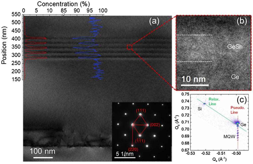
Figure 1.(a) Cross-sectional transmission electron microscopy (TEM) image of the MQW structure grown on the Si substrate with a Ge cap layer; the inset below is the selected-area diffraction pattern of the well layer; the inset above shows EDX linear scanning of elemental contents in the GeSn/Ge quantum well structure. The red and blue lines represent Sn and Ge concentrations, respectively. (b) HR-TEM image of the QW interface. (c) XRD-RSM from the () plane of the MQW structure.
3. DEVICE FABRICATION AND CHARACTERIZATION
Before the lithography process, a 300 nm thick layer was deposited on the film by plasma-enhanced chemical vapor deposition (PECVD). The GeSn/Ge MQWs films covered with a hard mask were patterned into a ridge waveguide with a size of (length) along the (110) crystal orientation. Subsequently, both sides of the GeSn/Ge MQW ridge waveguide were implanted into boron and phosphorous ions with an energy of 30 keV and a dose of . After ion implantation, in order to activate the implanted ions and repair the lattice damage caused by the ion implantation, the film was thermally annealed at 500°C for 10 s in the atmosphere. A micro-region Raman test shows that the lattice was recovered successfully. The 300 nm thick on the ridge waveguide was removed by wet etching, and then a thick surface passivation layer was deposited. Metal contacts were formed with a 100 nm thick nickel (Ni) layer to form a low-resistance metallic NiGe layer followed by an 800/50/50 nm thick aluminum (Al)/titanium (Ti)/gold (Au) layer deposition. Finally, in order to facilitate cleavage, the sample was thinned to 80 μm, and then the GeSn/Ge MQW ridge waveguide LEDs with different lengths were cleaved to expose (110) facets. The schematic diagram of the horizontal MQW ridge waveguide LEDs on the Si (100) substrate is shown in Fig. 2(a). Because the thickness of the MQW structure is very small and difficult to understand, a clearer cross-sectional schematic of this horizontal device is shown in Fig. 2(b). In addition, Fig. 2(c) is an oblique scanning electron microscope (SEM) image of the device. It can be seen that the cleaved facet is very neat and smooth.

Figure 2.(a) Schematic of horizontal GeSn/Ge MQW ridge waveguide LEDs on a Si (100) substrate. (b) Cross-sectional schematic of this horizontal device. (c) Scanning electron microscope (SEM) image of the ridge waveguide LEDs device. (d) Typical I-V characteristics of the device; inset: the relationship between and and the fitted curve of ideal factor .
Figure 2(d) shows the typical I-V characteristics of the device measured by the Agilent B1500A semiconductor parameter analyzer. The room temperature I-V curve shows well-defined rectifying behavior. The ideal factor can be obtained by the junction current-voltage formula [22]: , where is reverse saturated current, is elementary charge, is the Boltzmann constant, and is the absolute temperature. It can be seen from the inset in Fig. 2(d) that when the voltage is less than 0.5 V, the slope of the fitted line is about 17.97, and the ideal factor can be calculated to be about 2.1, which indicates that the main current of the junction is recombination current [23], and our device has an excellent carrier-injecting efficiency. Unlike vertical structure LEDs with the electrode on a Si substrate, the injection current of this horizontal device does not have to pass through the more defective Si/Ge interface. It means that the non-radiative recombination caused by the defects is greatly reduced.
EL measurements were performed using a standard off-axis configuration with a lock-in technique (optically chopped at 210 Hz) at room temperature. The light output power was collected by a Princeton Instruments SP-2300 spectrometer in step scan mode and a liquid nitrogen-cooled InGaAs detector with a cut-off wavelength of 2.4 μm. The EL spectra of the MQW ridge waveguide LED with a length of 1 mm are shown in Fig. 3(a). A strong emission peak located at 2160 nm (0.574 eV) with a full-width-at-half-maximum (FWHM) of is observed under a different power density. Since some of the injected carriers are recombined in a tensile strained Ge-buffer and Ge cap layer, a weaker emission peak can be seen at a wavelength of . The EL peak positions and intensity of these two peaks (main peaks and emission peaks of Ge) are displayed in Fig. 3(b) as a function of the power density. It can be seen from Fig. 2(b) that the intensity of both the emission peaks of Ge and the main peaks increases as the power density increases, and the intensity of the MQW structure is enhanced more significantly. In addition, both peaks gradually shift to longer wavelengths with increasing power density. This is because the Joule heat generated inside the device under a large injection current causes the device temperature to rise, resulting in bandgap shrinkage [24,25]. The PL of the as-grown sample and the EL of the device are compared, as shown in Fig. 3(c). The EL peak position (Peak 2) is consistent with the PL peak, indicating that the GeSn/Ge MQWs can remain stable for 10 s at an activation temperature of 500°C and do not deteriorate the quality of the material.
Figure 3.(a) EL spectra of horizontal MQW ridge waveguide LEDs at room temperature with different power density. (b) EL spectral peak wavelength as a function of power density. (c) PL spectrum of the as-grown sample and the EL spectrum of the device.
In order to investigate the confinement properties of MQW structures and analyze the mechanism of bandgap transition, the room-temperature band structure of the MQWs was theoretically calculated using the effective mass and six-band model [26], and the deformation potential theory is also used to calculate the effect of strain on the bandgap [27], as shown in Fig. 4(a). Table 1 shows the relevant parameters for the calculation of the energy bandgap of the GeSn alloy. As the composition of Sn in the alloy increases, it gradually transforms toward the direct bandgap material [11], and the compressive strain has an opposite effect [31]. It is known from Fig. 1 that the composition of Sn is approximately 9%, and the well layer is subjected to a compressive strain of 1.2%. Therefore, even the GeSn layer composition reaches , and it is still an indirect bandgap material. The calculation results show that the bandgap between -valley and -valley is only 5.2 meV. In the -valley () and heavy hole band (), their barrier heights are 142 meV and 111.5 meV, respectively. Therefore, these two barrier heights have sufficient confinement on the carriers. Using the finite-square potential well model, the first quantized energy level () and ground state () are calculated as 7 meV and 14 meV, respectively. At room temperature, carriers will transit from -valley to -valley due to a filling effect and fill the energy level [32]. Because the bandgap transition from to has a high recombination rate, the EL emission is dominated by the direct bandgap transition (). The bandgap between and is 0.573 eV, which is consistent with the EL peak position of 2160 nm (0.574 eV) in Fig. 3(a).
Figure 4.(a) Band diagram for one period of the quantum well by theoretical calculation. (b) Temperature-dependent PL spectra of the as-grown sample at the temperature range 80 K to 290 K.
| Material | Ev,av (eV) | av (eV) | acΓ (eV) | acL (eV) | Δ0 (eV) | b (eV) | EgΓ (eV) | EgL (eV) | C11 (GPa) | C12 (GPa) | bGeSnΓ (eV) | bGeSnL (eV) |
| Ge | 0 | 1.24 | −8.24 | −1.54 | 0.3 | −2.9 | 0.80 | 0.664 | 12.853 | 4.826 | 2.55 | 0.89 |
| Sn | 0.69 | 1.55 | −6 | −2.14 | 0.8 | −2.7 | −0.413 | 0.092 | 6.9 | 2.9 |
Table 1. Constants Used for Calculation of GeSn/Ge MQWs Energy Bandgap [27–30" target="_self" style="display: inline;">–30]
To further study the band-to-band transition in the MQWs, temperature-dependent PL measurements were performed, as shown in Fig. 4(b). Two peaks can be clearly observed within the temperature range of 110 K to 230 K, and both peaks shift toward shorter wavelengths as the temperature decreases. At 260 K and 290 K, only the high-energy peaks are visible. As the temperature decreases, two peaks can gradually be observed. For the high-energy peaks, the peak intensity decreases with decreasing temperature. On the contrary, the intensity of low-energy peaks increases instead. Because the thermal energy of the electrons decreases as the temperature decreases, the electrons do not have enough energy to occupy the energy level, so the emission of the indirect bandgap is more and more obvious. In addition, it can be seen that as the temperature decreases, the intensity of the low-energy peaks gradually increases, which is also because non-radiative recombination caused by defects is suppressed at low temperature [33,34]. And furthermore, the peak positions can be well matched with the band structure calculation in Fig. 4(a). The high-energy peak is mainly attributed to the transition, and the direct bandgap transition () also corresponds well to a low-energy peak. These results further illustrate the reliability of the band structure calculation in Fig. 4(a).
Figure 5 shows the current-output power of this device at room temperature measured by Thorlabs PM100D. As expected, the EL intensity monotonically increases with the injection current density from to . The dependence can be characterized by , where is EL intensity and is injection current density. The exponent can be used to characterize the emission mechanism. It can be seen that when the current density is less than , the exponent . This linear relationship indicates that the radiation recombination of the injected unbalanced carriers is dominant [35,36]. When , EL intensity is gradually saturated, which implies that the device has lower radiation recombination efficiency with very high injection current. Perhaps Auger recombination and light absorption by free carriers become stronger [37].
Figure 5.Output power of this device plotted as a function of at room temperature.
4. CONCLUSIONS
In summary, the horizontal GeSn/Ge MQW ridge waveguide LEDs were fabricated on Si (100) substrates to reduce the light absorption by metal electrodes and improve injection efficiency. The current-dependent EL spectra at room temperature exhibit a strong EL peak at a wavelength of (0.574 eV). The emission peaks remain stable at small injection currents without significant red-shift due to thermal effects. The device maintains high radiant recombination efficiency at low current densities (), and the light output power obtained was about 2.0 μW. Bandgap calculation results indicate that the MQWs form a type-I band alignment. The EL peak is in good agreement with the direct-bandgap transition (), and it can be verified by temperature-dependent PL spectra. These results indicate that GeSn/Ge MQWs are a potential candidate material for group-IV light sources, and such a horizontal structure experimentally proves that it has great potential as a Si-based light emitter. In addition, if the composition of Sn in the GeSn alloy is further increased, this material can be transformed into a direct-bandgap material. The EL performance of the device can be greatly improved and even achieve lasing.
References
[1] Q. Xu, B. Schmidt, S. Pradhan, M. Lipson. Micrometre-scale silicon electro-optic modulator. Nature, 435, 325-327(2005).
[2] F. Xia, L. Sekaric, Y. Vlasov. Ultracompact optical buffers on a silicon chip. Nat. Photonics, 1, 65-71(2006).
[3] S. Assefa, F. Xia, Y. A. Vlasov. Reinventing germanium avalanche photodetector for nanophotonic on-chip optical interconnects. Nature, 464, 80-84(2010).
[4] D. J. Richardson. Beating the electronics bottleneck. Nat. Photonics, 3, 562-564(2009).
[5] W. Song, R. Gatdula, S. Abbaslou, M. Lu, A. Stein, W. Y. Lai, J. Provine, R. F. Pease, D. N. Christodoulides, W. Jiang. High-density waveguide superlattices with low crosstalk. Nat. Commun., 6, 7027(2015).
[6] E. Timurdogan, C. M. Sorace-Agaskar, J. Sun, E. Shah Hosseini, A. Biberman, M. R. Watts. An ultralow power athermal silicon modulator. Nat. Commun., 5, 4008(2014).
[7] H. Chen, P. Verheyen, P. De Heyn, G. Lepage, J. De Coster, S. Balakrishnan, P. Absil, W. Yao, L. Shen, G. Roelkens, J. Van Campenhout. −1 V bias 67 GHz bandwidth Si-contacted germanium waveguide p-i-n photodetector for optical links at 56 Gbps and beyond. Opt. Express, 24, 4622-4631(2016).
[8] Z. Liu, J. Zhang, X. Li, L. Wang, J. Li, C. Xue, J. An, B. Cheng. 25 × 50 Gbps wavelength division multiplexing silicon photonics receiver chip based on a silicon nanowire-arrayed waveguide grating. Photon. Res., 7, 659-663(2019).
[9] M. V. Fischetti, S. E. Laux. Band structure, deformation potentials, and carrier mobility in strained Si, Ge, and SiGe alloys. J. Appl. Phys., 80, 2234-2252(1996).
[10] P. Moontragoon, Z. Ikonić, P. Harrison. Band structure calculations of Si–Ge–Sn alloys: achieving direct band gap materials. Semicond. Sci. Technol., 22, 742-748(2007).
[11] K. Lu Low, Y. Yang, G. Han, W. Fan, Y.-C. Yeo. Electronic band structure and effective mass parameters of Ge1-xSnx alloys. J. Appl. Phys., 112, 103715(2012).
[12] W. Huang, B. Cheng, C. Xue, Z. Liu. Comparative studies of band structures for biaxial (100)-, (110)-, and (111)-strained GeSn: a first-principles calculation with GGA+U approach. J. Appl. Phys., 118, 165704(2015).
[13] S. Gupta, B. Magyari-Köpe, Y. Nishi, K. C. Saraswat. Achieving direct band gap in germanium through integration of Sn alloying and external strain. J. Appl. Phys., 113, 073707(2013).
[14] W. Du, Y. Zhou, S. A. Ghetmiri, A. Mosleh, B. R. Conley, A. Nazzal, R. A. Soref, G. Sun, J. Tolle, J. Margetis, H. A. Naseem, S.-Q. Yu. Room-temperature electroluminescence from Ge/Ge1-xSnx/Ge diodes on Si substrates. Appl. Phys. Lett., 104, 241110(2014).
[15] B.-J. Huang, C.-Y. Chang, Y.-D. Hsieh, R. A. Soref, G. Sun, H.-H. Cheng, G.-E. Chang. Electrically injected GeSn vertical-cavity surface emitters on silicon-on-insulator platforms. ACS Photon., 6, 1931-1938(2019).
[16] Y. Zhou, W. Dou, W. Du, S. Ojo, H. Tran, S. A. Ghetmiri, J. Liu, G. Sun, R. Soref, J. Margetis, J. Tolle, B. Li, Z. Chen, M. Mortazavi, S.-Q. Yu. Optically pumped GeSn lasers operating at 270 K with broad waveguide structures on Si. ACS Photon., 6, 1434-1441(2019).
[17] S. Wirths, R. Geiger, N. von den Driesch, G. Mussler, T. Stoica, S. Mantl, Z. Ikonic, M. Luysberg, S. Chiussi, J. M. Hartmann, H. Sigg, J. Faist, D. Buca, D. Grützmacher. Lasing in direct-bandgap GeSn alloy grown on Si. Nat. Photonics, 9, 88-92(2015).
[18] D. Stange, N. von den Driesch, D. Rainko, C. Schulte-Braucks, S. Wirths, G. Mussler, A. T. Tiedemann, T. Stoica, J. M. Hartmann, Z. Ikonic, S. Mantl, D. Grutzmacher, D. Buca. Study of GeSn based heterostructures: towards optimized group IV MQW LEDs. Opt. Express, 24, 1358-1367(2016).
[19] D. Stange, N. von den Driesch, T. Zabel, F. Armand-Pilon, D. Rainko, B. Marzban, P. Zaumseil, J.-M. Hartmann, Z. Ikonic, G. Capellini, S. Mantl, H. Sigg, J. Witzens, D. Grützmacher, D. Buca. GeSn/SiGeSn heterostructure and multi quantum well lasers. ACS Photon., 5, 4628-4636(2018).
[20] G. T. Reed, M. R. Watts, Y.-L. Lin, Y.-H. Huang, S.-W. Chen, G.-E. Chang. GeSn waveguide structures for efficient light detection and emission. Proc. SPIE, 9367, 93671G(2015).
[21] Z. Liu, B.-W. Cheng, Y.-M. Li, C.-B. Li, C.-L. Xue, Q.-M. Wang. Effects of high temperature rapid thermal annealing on Ge films grown on Si(001) substrate. Chin. Phys. B, 22, 116804(2013).
[22] C. Popescu, J. C. Manifacier, R. Ardebili. I-V curve shape factor for thin p-n junctions at high injection levels. Phys. Status Solidi A, 158, 611-621(1996).
[23] C. T. Sah, R. N. Noyce, W. Shockley. Carrier generation and recombination in P-N junctions and P-N junction characteristics. Proc. IRE, 45, 1228-1243(1957).
[24] V. R. D’Costa, D. Schmidt, W. Wang, Y.-C. Yeo. Temperature dependence of the dielectric function and interband transitions of pseudomorphic GeSn alloys. J. Vac. Sci. Technol. B, 34, 041204(2016).
[25] Y. P. Varshni. Temperature dependence of the energy gap in semiconductors. Physica, 34, 149-154(1967).
[26] S. L. Chuang. Physics of Optoelectronic Devices(1995).
[27] C. G. Van de Walle. Band lineups and deformation potentials in the model-solid theory. Phys. Rev. B, 39, 1871-1883(1989).
[28] H. Pérez Ladrón de Guevara, A. G. Rodríguez, H. Navarro-Contreras, M. A. Vidal. Nonlinear behavior of the energy gap in Ge1-xSnx alloys at 4K. Appl. Phys. Lett., 91, 161909(2007).
[29] W.-J. Yin, X.-G. Gong, S.-H. Wei. Origin of the unusually large band-gap bowing and the breakdown of the band-edge distribution rule in the SnxGe1-x alloys. Phys. Rev. B, 78, 161203(2008).
[30] N. Yahyaoui, N. Sfina, J. L. Lazzari, A. Bournel, M. Said. Band engineering and absorption spectra in compressively strained Ge0.92Sn0.08/Ge (001) double quantum well for infrared photodetection. Phys. Stat. Solidi C, 11, 1561-1565(2014).
[31] A. A. Tonkikh, C. Eisenschmidt, V. G. Talalaev, N. D. Zakharov, J. Schilling, G. Schmidt, P. Werner. Pseudomorphic GeSn/Ge(001) quantum wells: examining indirect band gap bowing. Appl. Phys. Lett., 103, 032106(2013).
[32] X. Sun, J. Liu, L. C. Kimerling, J. Michel. Direct gap photoluminescence of n-type tensile-strained Ge-on-Si. Appl. Phys. Lett., 95, 032106(2009).
[33] M.-Y. Ryu, T. R. Harris, Y. K. Yeo, R. T. Beeler, J. Kouvetakis. Temperature-dependent photoluminescence of Ge/Si and Ge1-ySny/Si, indicating possible indirect-to-direct bandgap transition at lower Sn content. Appl. Phys. Lett., 102, 171908(2013).
[34] W. Du, S. A. Ghetmiri, B. R. Conley, A. Mosleh, A. Nazzal, R. A. Soref, G. Sun, J. Tolle, J. Margetis, H. A. Naseem, S.-Q. Yu. Competition of optical transitions between direct and indirect bandgaps in Ge1-xSnx. Appl. Phys. Lett., 105, 051104(2014).
[35] W. H. Chang, A. T. Chou, W. Y. Chen, H. S. Chang, T. M. Hsu, Z. Pei, P. S. Chen, S. W. Lee, L. S. Lai, S. C. Lu, M. J. Tsai. Room-temperature electroluminescence at 1.3 and 1.5 μm from Ge/Si self-assembled quantum dots. Appl. Phys. Lett., 83, 2958-2960(2003).
[36] Z. Liu, W. Hu, C. Li, Y. Li, C. Xue, C. Li, Y. Zuo, B. Cheng, Q. Wang. Room temperature direct-bandgap electroluminescence from n-type strain-compensated Ge/SiGe multiple quantum wells. Appl. Phys. Lett., 101, 231108(2012).
[37] G. Sun, R. A. Soref, H. H. Cheng. Design of an electrically pumped SiGeSn/GeSn/SiGeSn double-heterostructure midinfrared laser. J. Appl. Phys., 108, 033107(2010).


