• Chinese Optics Letters
  • Vol. 21, Issue 6, 061301 (2023)
Zixian Guo, Bei Yan, and Jianjun Liu*
Author Affiliations
  • Key Laboratory for Micro/Nano Optoelectronic Devices of Ministry of Education & Hunan Provincial Key Laboratory of Low-Dimensional Structural Physics and Devices, School of Physics and Electronics, Hunan University, Changsha 410082, China
  • show less
    DOI: 10.3788/COL202321.061301 Cite this Article Set citation alerts
    Zixian Guo, Bei Yan, Jianjun Liu. Photonic and phononic interface states based on sunflower-type crystals [Invited][J]. Chinese Optics Letters, 2023, 21(6): 061301 Copy Citation Text show less

    Abstract

    Interface states are widely applied in waveguide devices. However, previous studies failed to achieve photonic and phononic interface states independent of each other in the same crystal structure depending on the behavior of the crystal structure, i.e., photonic or phononic crystals, making the function of interface states single. In this study, straight-line and circular photonic and phononic interface states were realized independently in sunflower-type crystals. In addition, with a defect and a metal barrier, interface states could remain almost undamaged. The results have the potential to achieve multi-function devices and reduce the cost of engineering applications.

    1. Introduction

    Photonic crystals (PCs)[1,2] [phononic crystals (PnCs)[3]] are artificial microstructures in which dielectric constants (density and elastic moduli) are arranged in periodic or quasi-periodic order. When electromagnetic waves (elastic waves) propagate inside PCs (PnCs), waves in a certain frequency region cannot propagate due to the internal structure, that is, a bandgap (BG) is formed. The BG can be changed and thus regulated by adjusting the material or structure of PCs (PnCs). PCs and PnCs offer broad application prospects in the fields of filters[4,5], isolators[6,7], sensors[810], lenses[1114], resonators[15,16], lasers[17,18], etc.

    Interface states can be used to regulate the propagation of waves, and they are widely applied in waveguide devices[1921]. For PCs, the condition to realize interface states is that, in a common BG, there exists a frequency region where the sum of surface impedances is zero[22]. Based on this, one-dimensional (1D) interface states were realized[23], and then interface states were expanded to two-dimensional (2D) periodic square lattice PCs when two kinds of dielectric cylinders with the interchange of their materials of background and dielectric cylinders are arranged in mirror symmetry[24,25]. Further, interface states were expanded from straight-line to circular shape, which indicated the change in propagation direction to curved paths[26]. Thereafter, interface states were also realized in rectangular lattices[27]. PnCs possess the similar property of band manipulation to PCs, and interface states can also be realized in 1D periodic PnCs[28,29]. However, it was difficult to guarantee the complete translational symmetry of the structure in the actual preparation process. As a result, researchers introduced quasi-periodic structures and realized interface states in phononic quasi-crystals[30]. According to previous studies[1931], most structures capable of realizing interface states can only allow the transmission of electromagnetic waves or elastic waves alone and thus the function of relevant devices is limited, especially structures without translational symmetry. In order to realize photonic and phononic interface states independently in the same nontranslationally symmetric crystal structure, construction of a workable structure is required. Photonic and phononic phenomena realized in the same structure are used in many devices, such as filters[32,33], microcavities[34,35], and sensors[36]. Combined electromagnetic and elastic waves can also be used for detecting nonmetallic buried objects[37], or creating optical isolation by means of elastic waves in an optical waveguide[38]. In order to enrich the function of interface states and reduce the cost of device preparation, it is urgent to research the achievement of photonic and phononic interface states independent of each other in the same structure, which can be used to carry different information, remove interferences, and retain useful signals.

    In this study, photonic and phononic interface states were realized independently in the same crystal structure at the interface of two inverted square lattices (the materials of their background and cylinders were interchanged). By using the same material and structural parameters, the upper–lower and the inner–outer combination structures of sunflower-type crystals were constructed. When electromagnetic waves and elastic waves are incident, respectively, periodic modes propagating along the interface appear, which indicates that both photonic and phononic interface states can be realized independently in this structure. The interface states realized in sunflower-type crystals are possessed with good robustness and can be output from any angle.

    2. Structural Design and Theoretical Aspects

    Sunflower-type PCs (PnCs) exhibit periodicity in circular direction, which can be regarded as the translational symmetry in a polar coordinate system. The position of each dielectric (elastic) cylinder can be expressed as follows: x=aNcos(2nπ/6N),y=aNsin(2nπ/6N),n=1 to 6N,where a is the lattice constant, N is the ordinal of the ring (N starts from 1 without including the centric cylinder of the entire structure), and n denotes the ordinal of a certain cylinder in the Nth ring. Equation (1) indicates that in the Nth circle, the angle is 2π/6N when two adjacent cylinders are connected to the center of the entire sunflower-type crystal. In addition, the number of cylinders in each circle is 6N. Based on this, two types of sunflower-type crystals with interchangeable materials can be constructed, as shown in Figs. 1(a) and 1(b). When the interface is required to be straight-line and circular, respectively, the upper–lower and inner–outer combination structures of sunflower-type crystals can be constructed, as shown in Figs. 1(c) and 1(d).

    The sunflower-type crystal and its combination structures. (a) Radius of crystal with glass as dielectric (elastic) cylinders, r1 = 0.5a; (b) radius of crystal with water as dielectric (elastic) cylinders, r2 = 0.3a; (c) upper–lower combination structure; (d) inner–outer combination structure. The parameters of glass (gray) and water (blue) are as follows: relative dielectric constant εr1 = 3.75 and εr2 = 78.5; bulk modulus K1 = 3.7 × 10¹⁰ and K2 = 2.2 × 10⁹; density ρ1 = 2500 kg m−3 and ρ2 = 1000 kg m−3. The zoom-in schematics of these four structures are attached to the upper right corners.

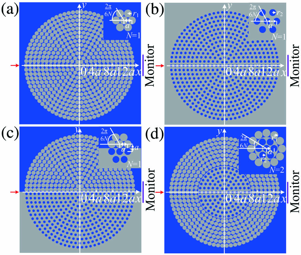
    Figure 1.The sunflower-type crystal and its combination structures. (a) Radius of crystal with glass as dielectric (elastic) cylinders, r1 = 0.5a; (b) radius of crystal with water as dielectric (elastic) cylinders, r2 = 0.3a; (c) upper–lower combination structure; (d) inner–outer combination structure. The parameters of glass (gray) and water (blue) are as follows: relative dielectric constant εr1 = 3.75 and εr2 = 78.5; bulk modulus K1 = 3.7 × 10¹⁰ and K2 = 2.2 × 10⁹; density ρ1 = 2500 kg m−3 and ρ2 = 1000 kg m−3. The zoom-in schematics of these four structures are attached to the upper right corners.

    Sensors and optical fiber devices based on sunflower-type crystals exhibit fascinating characteristics, such as high sensitivity and high propagation efficiency[39]. Moreover, sunflower-type PCs and PnCs also show good application prospects in lasers[40], microcavities[41], curved waveguides[42], and one-way rotating state devices[43]. The realization of interface states in sunflower-type crystals can expand their application fields.

    In structures with translational symmetry, two types of PCs need to have a common BG to realize interface states. Within the common BG, there must be a region satisfying the condition that the sum of surface impedances is zero.

    That is, Z1(ω,ky)+Z2(ω,ky)=0,where Z1(ω,ky) and Z2(ω,ky) are surface impedances of two types of PCs under given ω and ky, respectively, which are defined as follows: Z1=Ex(z=0)/Hy(z=0),Z2=Ex(z=0+)/Hy(z=0+).

    The interface of two PCs is marked as z=0. The surface impedance is related to the reflection coefficient r and the transmission coefficient t. The relation between them is defined as follows: Z(ω,ky)=±(1+r)2t2(1r)2t21ky2/k2,where k is the amplitude of wave vector k, and ky is the tangential component of k along the interface. When incident waves are located in the BG and perpendicularly incident to the surface of PCs, total reflection occurs. At this time, the surface impedance has nothing to do with the transmission coefficient and can be reduced to a pure imaginary number.

    When the imaginary part of the surface impedance is negative (positive), the surface impedance decreases (increases) monotonically from zero (positive infinity) to negative infinity (zero) with the increase in the frequency. Based on this, when imaginary parts of surface impedances in the common BG of two PCs are opposite (one is positive and the other is negative), there must be a certain frequency where the sum of surface impedances is zero [Eq. (2)], that is, a deterministic interface state is generated[24]. Therefore, to verify the generation of interface states, the imaginary part of the surface impedance of each BG should be obtained.

    PCs and PnCs exhibit high similarities in the manipulation of bands; thus the interface states in PnCs need to satisfy the condition of surface impedance[2830]. Based on the theory of surface impedance, deterministic interface states in PCs with translational symmetry can be realized by combining inverted PCs. Similarly, interface states can also be realized when inverted PnCs are combined. Therefore, under the same material and structural parameters, photonic and phononic interface states can be realized independently in the same structure. By combining these two inverted PCs (PnCs), the interface state can be generated in the common BG.

    Based on previous studies[22,44], imaginary parts of surface impedances of two adjacent BGs are related to the Zak phase of the band between them, which can be expressed as follows: Sgn[Im(Zn(ω,ky))]Sgn[Im(Zn1(ω,ky))]=ei(ψn1+π),where ψn1 represents the Zak phase of the (n1)th band. The Zak phase in the 1D band can only be 0 or π. Considering the center of the Brillouin zone or the midpoint of the left boundary of the unit cell as the calculating center, the Zak phase can be obtained according to the symmetry of electric field distribution of the two high symmetry points of the band[22]. The imaginary part of surface impedance of each BG can be obtained from Eq. (6), with the lowest BG being negative. When two types of PCs (PnCs) have opposite signs in the common BG, the realization of interface states can be proven.

    3. Results and Discussion

    In order to find appropriate parameters that could be applied in sunflower-type crystals, photonic and phononic interface states in the same square lattice were first realized independently. In Fig. 2, the combination structures of two kinds of square lattice [one with glass as dielectric (elastic) cylinders and the other with water as dielectric (elastic) cylinders] are calculated, with the radius shown in Fig. 1. For the square lattice PCs with glass (water) as dielectric cylinders and water (glass) as background, the projected band structures are the green (blue) color lines, as shown in Fig. 2(a). An additional band appears at the common BG when these two types of PCs are combined into a complete structure. The same phenomenon occurs with PnCs shown in Fig. 2(b). This indicates that, in the original frequency range where waves cannot propagate in these two types of PCs (PnCs), a propagable state is generated after combination. This is denoted as the interface state and it is shown as red lines in Fig. 2. The results indicate that the interface state of square lattice PCs is generated in the region of fsquare_photonic[29.77GHz,33.51GHz], while that of PnCs is generated in the region of fsquare_phononic[0.92MHz,1.04MHz]. Photonic and phononic interface states can be realized independently in the same square lattice structure by adjusting the material and structural parameters of crystals. In order to directly exhibit the propagation characteristics of interface states in square lattices, the distributions of electric field and sound pressure field were calculated by the finite-element method in 2D simulation. The port is set at the left boundary and covers a range of one dielectric (elastic) cylinder. Electromagnetic (elastic) waves are incident from the port with initial value E=1V (P=1Pa) and the simulation is set at the temperature of 273.15 K and pressure of 1.013 × 10⁵ Pa. The results are shown in Fig. 3.

    Projected band structures. Interface states are expressed in red lines, and bands of square lattice are expressed in green lines [with glass as dielectric cylinders in (a) and elastic cylinders in (b)] and blue lines [with water as dielectric cylinders in (a) and elastic cylinders in (b)]: (a) PCs; (b) PnCs.

    Figure 2.Projected band structures. Interface states are expressed in red lines, and bands of square lattice are expressed in green lines [with glass as dielectric cylinders in (a) and elastic cylinders in (b)] and blue lines [with water as dielectric cylinders in (a) and elastic cylinders in (b)]: (a) PCs; (b) PnCs.

    Electric field (sound pressure field) distribution when electromagnetic (elastic) waves propagate in the combined structure of two types of PCs (PnCs). (a) PCs at f = 30.6 GHz; (b) PnCs at f = 0.96 MHz. The material of bigger cylinders is glass, and the background material is water. The material of smaller cylinders is water, and the background material is glass. The parameters of glass and water are shown in Fig. 1.

    Figure 3.Electric field (sound pressure field) distribution when electromagnetic (elastic) waves propagate in the combined structure of two types of PCs (PnCs). (a) PCs at f = 30.6 GHz; (b) PnCs at f = 0.96 MHz. The material of bigger cylinders is glass, and the background material is water. The material of smaller cylinders is water, and the background material is glass. The parameters of glass and water are shown in Fig. 1.

    The electric field and sound pressure field are distributed periodically along the boundary and decay rapidly on both sides of the boundary. It indicates that the photonic and phononic interface states are realized independently in this square lattice structure. The advantages of propagation are reflected.

    In this study, material and structural parameters in a square lattice were applied to the upper–lower and inner–outer combination structures of sunflower-type crystals. Then the transmission spectra, electric field, and sound pressure field distributions were calculated to analyze the realization of straight-line and circular interface states in sunflower-type PCs and PnCs.

    When the upper–lower combination structure of sunflower-type crystals is constructed according to Fig. 1(c) and electromagnetic waves are incident on the left port, the structure is used as PCs. When incident waves are elastic waves, the structure is used as PnCs. In order to find out whether interface states can exist in the upper–lower combination structure of sunflower-type crystals, we calculated the transmission spectra of two types of sunflower-type crystals, respectively, and the upper–lower combination structure of the sunflower-type crystals.

    The transmission spectra of PCs and PnCs are shown in Fig. 4. Figure 4(a) demonstrates that when electromagnetic waves are incident, this structure is used as PCs. BGs of two types of sunflower-type PCs are f1photonic[27GHz,36.1GHz] and f2photonic[25.7GHz,37.4GHz], respectively. The common BG of the two PCs is fCphotonic[27GHz,36.1GHz], as indicated in Fig. 4(a). When elastic waves are incident, this structure is used as PnCs. BGs of two types of sunflower-type PnCs are f1phononic[0.84MHz,1.29MHz], f2phononic[0.79MHz,1.44MHz], respectively. The common BG of the two PnCs is fCphononic[0.84MHz,1.29MHz], as indicated in Fig. 4(b). The transmission spectra of the upper–lower combination structures of sunflower-type crystals are shown in Figs. 4(c) and 4(d), respectively. In the transmission spectrum of PCs (PnCs), some transmission peaks appear in the region of ful_photonic[29.05GHz,33.3GHz] (ful_phononic[0.91MHz,1.04MHz]), which belongs to the region of fCphotonic (fCphononic).

    Transmission spectra of models shown in Figs. 1(a) and 1(b). (a) PCs; (b) PnCs. Transmission spectra of the model shown in Fig. 1(c) [the radius of upper (lower) cylinders is r1 = 0.5a (r2 = 0.3a)]: (c) PCs; (d) PnCs.

    Figure 4.Transmission spectra of models shown in Figs. 1(a) and 1(b). (a) PCs; (b) PnCs. Transmission spectra of the model shown in Fig. 1(c) [the radius of upper (lower) cylinders is r1 = 0.5a (r2 = 0.3a)]: (c) PCs; (d) PnCs.

    The result indicates that some propagable states are generated after combination, that is, interface states are generated. The propagation constant k of waves at different frequencies is different, resulting in different modes. The phenomena in the upper–lower combination structures of sunflower-type crystals are consistent with the phenomena in the square lattice. With the same simulation environment and setting conditions shown in Fig. 3, the distributions of the electric field and sound pressure field are shown in Fig. 5. Figure 5 demonstrates that irrespective of PCs or PnCs, the distributions of the electric field and sound pressure field are periodic along the boundary as in the square lattice. It shows that photonic and phononic interface states can be realized independently in the upper–lower combination structure of sunflower-type crystals. The arrangements of dielectric (elastic) cylinders in the square lattice and the upper–lower combination structure of sunflower-type crystals [Fig. 1(c)] both show a mirror symmetry on average along the boundary. According to the inner–outer combination structure of sunflower-type crystals shown in Fig. 1(d), the mirror symmetry is broken and the translational symmetry in the rectangular coordinate system is transformed into the translational symmetry in the polar coordinate system (that is, the rotational symmetry). In order to find out whether interface states can exist in structures with rotational symmetry rather than translational symmetry, the transmission spectra of the inner–outer combination structure of sunflower-type crystals are calculated in Fig. 6, respectively.

    Considering Fig. 1(c) as the model, the field distributions of the upper–lower combination structure of sunflower-type crystals. (a) PCs at f = 30.54 GHz; (b) PnCs at f = 0.96 MHz.

    Figure 5.Considering Fig. 1(c) as the model, the field distributions of the upper–lower combination structure of sunflower-type crystals. (a) PCs at f = 30.54 GHz; (b) PnCs at f = 0.96 MHz.

    Transmission spectra of models shown in Fig. 1(d) [the radius of outer (inner) cylinders is r1 = 0.5a (r2 = 0.3a)]. (a) PCs; (b) PnCs.

    Figure 6.Transmission spectra of models shown in Fig. 1(d) [the radius of outer (inner) cylinders is r1 = 0.5a (r2 = 0.3a)]. (a) PCs; (b) PnCs.

    As shown in Fig. 6, transmission peaks appear in the region of fio_photonic[29.05GHz,33.3GHz] (fio_phononic[0.91MHz,1.06MHz]), which belongs to the region of fCphotonic (fCphononic). Frequencies of transmission peaks occurring in the BG are selected to calculate the distributions of electric field and sound pressure field, as shown in Fig. 7. Both the electric field and the sound pressure field are distributed periodically along the circular interface, and decay rapidly as they extend to the interior of the crystal on both sides. The transmission spectra of PCs and PnCs [Figs. 6(a) and 6(b)], and the field distribution [Figs. 7(a) and 7(b)] analysis indicate that photonic and phononic interface states can still be realized in the inner–outer combination structure of sunflower-type crystals.

    Considering Fig. 1(d) as the model, the field distributions of the inner–outer combination structure of sunflower-type crystals. (a) Electric field of PCs at f = 30.54 GHz; (b) sound pressure field of PnCs at f = 0.96 MHz.

    Figure 7.Considering Fig. 1(d) as the model, the field distributions of the inner–outer combination structure of sunflower-type crystals. (a) Electric field of PCs at f = 30.54 GHz; (b) sound pressure field of PnCs at f = 0.96 MHz.

    In the application process of PCs and PnCs, due to the limitations of the preparation technology or the loss in the use process, the crystal structure may be incomplete, defective, or obstructed. Therefore, we explored the formation of interface states of the inner–outer combination structure of sunflower-type crystals with a defect and a metal barrier, as shown in Figs. 8 and 9.

    Transmission spectra of PCs and PnCs with a defect and a metal barrier. (a) PCs; (b) PnCs.

    Figure 8.Transmission spectra of PCs and PnCs with a defect and a metal barrier. (a) PCs; (b) PnCs.

    Field distributions of the inner–outer combination structure of sunflower-type crystals with (a), (b) a defect and (c), (d) a metal barrier. (a) Electric field of PCs at f = 30.54 GHz; (b) sound pressure field of PnCs at f = 0.96 MHz; (c) electric field of PCs at f = 30.54 GHz; (d) sound pressure field of PnCs at f = 0.96 MHz.

    Figure 9.Field distributions of the inner–outer combination structure of sunflower-type crystals with (a), (b) a defect and (c), (d) a metal barrier. (a) Electric field of PCs at f = 30.54 GHz; (b) sound pressure field of PnCs at f = 0.96 MHz; (c) electric field of PCs at f = 30.54 GHz; (d) sound pressure field of PnCs at f = 0.96 MHz.

    The transmission spectra of PCs and PnCs with a defect and a metal barrier are shown in Fig. 8. Irrespective of defect (represented by red lines) or metal barrier (represented by blue lines), transmission peaks exist in the region of fdm_photonic[29.05GHz,33.3GHz] (fdm_phononic[0.91MHz,1.06MHz]) where interface states of the complete inner–outer combination structures of sunflower-type PCs (PnCs) exist.

    As shown in Figs. 9(a) and 9(b), when a dielectric (an elastic) cylinder is removed from the crystal, the completeness is damaged, while the electromagnetic (elastic) waves can still propagate along the interface. That is to say, interface states are almost undamaged. When a metal barrier is inserted at the interface of the crystal, the barrier cannot prevent the formation of interface states, as shown in Figs. 9(c) and 9(d). The transmission spectra and field distributions show that interface states possess good robustness.

    Sunflower-type crystals can make interface states realized as a circular shape, which allows electromagnetic waves or elastic waves to be output from any angle when the input port is determined. The results shown in Fig. 10 are output from angles of 120°, 90°, and 60°, respectively. To achieve the same angular output in square lattices, it is necessary to use straight waveguides with obtuse, right, and acute angles, which may cause greater loss when waves propagate through these angles and even destroy interface states.

    Field distributions of output from angles of 120°, 90°, and 60°. (a) Electric field of PCs at f = 30.54 GHz; (b) sound pressure field of PnCs at f = 0.96 MHz.

    Figure 10.Field distributions of output from angles of 120°, 90°, and 60°. (a) Electric field of PCs at f = 30.54 GHz; (b) sound pressure field of PnCs at f = 0.96 MHz.

    4. Conclusion

    Based on the material and structural parameters that could realize photonic and phononic interface states independently in the same square lattice, interface states in PCs and PnCs were realized independently in the upper–lower and inner–outer combination structures of sunflower-type crystals. For these crystal types, materials of background and dielectric (elastic) cylinders were interchanged, which enabled the independent realization of straight-line or circular photonic and phononic interface states in the same sunflower-type crystals. These interface states are possessed with good robustness and can be output from any angle. This result can expand the function of waveguides, filters, isolators, and so on, realizing the dual use of devices and reducing the cost of production.

    References

    [1] E. Yablonovitch. Inhibited spontaneous emission in solid-state physics and electronics. Phys. Rev. Lett., 58, 2059(1987).

    [2] S. John. Strong localization of photons in certain disordered dielectric superlattices. Phys. Rev. Lett., 58, 2486(1987).

    [3] M. S. Kushwaha, P. Halevi, L. Dobrzynski, B. Djafari-Rouhani. Acoustic band structure of periodic elastic composites. Phys. Rev. Lett., 71, 2022(1993).

    [4] Y. F. Zhao, Z. M. Wang, Z. J. Jiang, C. X. Yue, X. Chen, J. Z. Wang, J. J. Liu. Add-drop filter with compound structures of photonic crystal and photonic quasicrystal. J. Infrared Millim. Waves, 36, 342(2017).

    [5] A. H. M. Almawgani, D. N. Alhamss, S. A. Taya, I. Colak, A. Sharma, A. R. H. Alhawari, S. K. Patel. The properties of a tunable terahertz filter based on a photonic crystal with a magnetized plasma defect layer. Phys. Fluids, 34, 082020(2022).

    [6] Y. Wang, B. Xu, D. Zhang, S. Xu, Z. Dong, X. Zeng, X. Lu, J. Pei. Magneto-optical isolator based on ultra-wideband photonic crystals waveguide for 5G communication system. Crystals, 9, 570(2019).

    [7] Y. Jin, X. Y. Jia, Q. Q. Wu, X. He, G. C. Yu, L. Z. Wu, B. L. Luo. Design of vibration isolators by using the Bragg scattering and local resonance band gaps in a layered honeycomb meta-structure. J. Sound Vib., 521, 116721(2022).

    [8] R. Ge, J. Xie, B. Yan, E. Liu, W. Tan, J. Liu. Refractive index sensor with high sensitivity based on circular photonic crystal. J. Opt. Soc. Am. A, 35, 992(2018).

    [9] A. Shi, R. Ge, J. Liu. Refractive index sensor based on photonic quasi-crystal with concentric ring microcavity. Superlattices Microst., 133, 106198(2019).

    [10] A. Shi, R. Ge, J. Liu. Side-coupled liquid sensor and its array with magneto-optical photonic crystal. J. Opt. Soc. Am. A, 37, 1244(2020).

    [11] Z. Tan, Y. Wei, Y. Tian, X. Han. Gradient negative refraction index phononic crystal lens with a rotating scatterer. Mater. Res. Express, 6, 096203(2019).

    [12] J. Sheng, J. Xie, J. Liu. Multiple super-resolution imaging in the second band of gradient lattice spacing photonic crystal flat lens. Chin. Opt. Lett., 18, 120501(2020).

    [13] H. Zhao, J. Xie, J. Liu. Optical and acoustic super-resolution imaging in a Stampfli-type photonic quasi-crystal flat lens. Results Phys., 27, 104537(2021).

    [14] T. X. Ma, Z. Y. Li, C. Z. Zhang, Y. S. Wang. Energy harvesting of Rayleigh surface waves by a phononic crystal Luneburg lens. Int. J. Mech. Sci., 227, 107435(2022).

    [15] S. P. Yu, D. C. Cole, H. Jung, G. T. Moille, K. Srinivasan, S. B. Papp. Spontaneous pulse formation in edgeless photonic crystal resonators. Nat. Photonics, 15, 461(2021).

    [16] F. Gao, A. Bermak, S. Benchabane, L. Robert, A. Khelif. Acoustic radiation-free surface phononic crystal resonator for in-liquid low-noise gravimetric detection. Microsyst. Nanoeng., 7, 8(2021).

    [17] Y. Huang, T. Zhou, M. Tang, G. Xiang, H. Li, M. Martin, T. Baron, S. Chen, H. Liu, Z. Zhang. Highly integrated photonic crystal bandedge lasers monolithically grown on Si substrates. Chin. Opt. Lett., 20, 041401(2022).

    [18] J. Liu, M. Wang, Y. Wang, X. Zhou, T. Fu, A. Qi, H. Qu, X. Xing, W. Zheng. High peak power density and low mechanical stress photonic-band-crystal diode laser array based on non-soldered packaging technology. Chin. Opt. Lett., 20, 071403(2022).

    [19] Q. Cheng, Y. Pan, Q. Wang, T. Li, S. Zhu. Topologically protected interface mode in plasmonic waveguide arrays. Laser Photon. Rev., 9, 392(2015).

    [20] Y. Yang, T. Xu, Y. F. Xu, Z. H. Hang. Zak phase induced multiband waveguide by two-dimensional photonic crystals. Opt. Lett., 42, 3085(2017).

    [21] W. Song, W. Sun, C. Chen, Q. Song, S. Xiao, S. Zhu, T. Li. Integrated photonic devices: robust and broadband optical coupling by topological waveguide arrays. Laser Photonics Rev., 14, 1900193(2020).

    [22] X. Huang, M. Xiao, Z. Q. Zhang, C. T. Chan. Sufficient condition for the existence of interface states in some two-dimensional photonic crystals. Phys. Rev. B, 90, 075423(2014).

    [23] M. Xiao, Z. Q. Zhang, C. T. Chan. Surface impedance and bulk band geometric phases in one-dimensional systems. Phys. Rev. X, 4, 021017(2014).

    [24] X. Huang, Y. Yang, Z. H. Hang, Z. Q. Zhang, C. T. Chan. Geometric phase induced interface states in mutually inverted two-dimensional photonic crystals. Phys. Rev. B, 93, 085415(2016).

    [25] X. D. Chen, D. Zhao, X. S. Zhu, F. L. Shi, H. Liu, J. C. Lu, M. Chen, J. W. Dong. Edge states in self-complementary checkerboard photonic crystals: Zak phase, surface impedance, and experimental verification. Phys. Rev. A, 97, 013831(2018).

    [26] Z. Guo, B. Yan, J. Liu. Straight lined and circular interface states in sunflower-type photonic crystals. J. Opt., 22, 035002(2020).

    [27] J. Chen, J. Xie, E. Liu, B. Yan, J. Liu. Interface states in the rectangular lattice photonic crystals with identical dielectric rods. Results Phys., 23, 104082(2021).

    [28] Y. Meng, X. Wu, R. Y. Zhang, X. Li, P. Hu, L. Ge, Y. Huang, H. Xiang, D. Han, S. Wang, W. Wen. Designing topological interface states in phononic crystals based on the full phase diagrams. New J. Phys., 20, 073032(2018).

    [29] H. Zhang, B. Liu, X. Zhang, Q. Wu, X. Wang. Zone folding induced tunable topological interface states in one-dimensional phononic crystal plates. Phys. Lett. A, 383, 2797(2019).

    [30] J. Zhao, S. Huo, H. Huang, J. Chen. Topological interface states of shear horizontal guided wave in one-dimensional phononic quasicrystal slabs. Phys. Status Solidi Rapid Res. Lett., 12, 1800322(2018).

    [31] Q. Xu, Y. Peng, B. Yan, A. Shi, P. Peng, J. Xie, J. Liu. Multiband topological states in the Penrose-triangle photonic crystals. Opt. Lett., 48, 101(2023).

    [32] H. Li, W. Liu, T. Yu, T. Wang, Q. Liao. Simultaneous unidirectional reciprocal filters of electromagnetic and elastic waves based on the modal symmetry of phoxonic crystal waveguides and cavity. Phys. Lett. A, 384, 126499(2020).

    [33] S. Z. Aboutalebi, A. Bahrami. Design of phoxonic filter using locally-resonant cavities. Phys. Scr., 96, 075704(2021).

    [34] Z. Wang, W. Liu, T. Yu, T. Wang, H. Li, N. Liu, Q. Liao. Simultaneous localization of photons and phonons within the transparency bands of LiNbO3 phoxonic quasicrystals. Opt. Express, 24, 23353(2016).

    [35] T. Yu, Z. Wang, W. Liu, T. Wang, N. Liu, Q. Liao. Simultaneous large band gaps and localization of electromagnetic and elastic waves in defect-free quasicrystals. Opt. Express, 24, 7951(2016).

    [36] S. M. Shaban, A. Mehaney, A. H. Aly. Determination of 1-propanol, ethanol, and methanol concentrations in water based on a one-dimensions phoxonic crystal sensor. Appl. Opt., 59, 3878(2020).

    [37] W. Scott, J. Martin. An experimental model of an acousto-electromagnetic sensor for detecting land mines. Antennas and Propagation Society International Symposium(1998).

    [38] Z. Yu, S. Fan. Complete optical isolation created by indirect interband photonic transitions. Nat. Photonics, 3, 91(2009).

    [39] D. X. Yan, J. S. Li, Y. Wang. High sensitivity terahertz refractive index sensor based on sunflower-shaped circular photonic crystal. Acta Phys. Sin., 68, 207801(2019).

    [40] P. T. Lee, T. W. Lu, J. H. Fan, F. M. Tsai. High quality factor microcavity lasers realized by circular photonic crystal with isotropic photonic band gap effect. Appl. Phys. Lett., 90, 151125(2007).

    [41] X. Zhang, X. Sun, H. X. Tang. A 1.16-µm-radius disk cavity in a sunflower-type circular photonic crystal with ultrahigh quality factor. Opt. Lett., 37, 3195(2012).

    [42] W. Liu, X. H. Sun, Q. B. Fan, S. Wang, Y. L. Qi. The investigation of multi-channel splitters and big-bend waveguides based on 2D sunflower-typed photonic crystals. Superlattices Microst., 100, 1291(2016).

    [43] T. Hou, R. Ge, W. Tan, J. Liu. One-way rotating state of multi-periodicity frequency bands in circular photonic crystal. J. Phys. D Appl. Phys., 53, 075104(2020).

    [44] J. Zak. Berry’s phase for energy bands in solids. Phys. Rev. Lett., 62, 2747(1989).

    Zixian Guo, Bei Yan, Jianjun Liu. Photonic and phononic interface states based on sunflower-type crystals [Invited][J]. Chinese Optics Letters, 2023, 21(6): 061301
    Download Citation