Abstract
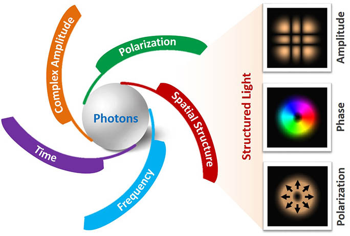
Metasurfaces and structured light have rapidly advanced over the past few years, from being paradigms to forming functional devices and tailoring special light beams for wide emerging applications. Here, we focus on harnessing metasurfaces for structured light manipulation. We review recent advances in shaping structured light by metasurfaces on different platforms (metal, silica, silicon, and fiber). Structured light manipulation based on plasmonic metasurfaces, reflection-enhanced plasmonic metasurfaces, metasurfaces on fiber facets, dielectric metasurfaces, and sub-wavelength structures on silicon are presented, showing impressive performance. Future trends, challenges, perspectives, and opportunities are also discussed.Different from electrons, photons feature multiple degrees of freedom, including frequency/wavelength, time, complex amplitude (amplitude, phase), polarization, and spatial structure. Manipulating these physical dimensions of photons enables a diversity of light related applications. Beyond the traditional attention to frequency, time, complex amplitude, and polarization, the spatial structure, which is the only known physical dimension left, has attracted increasing interest. Shaping the spatial structure of lightwaves enables the generation of various special light beams. Shown in Fig. 1 are typical examples of inhomogeneous amplitude, phase, and polarization distribution across the light beams, such as Hermite–Gaussian/Laguerre–Gaussian/Bessel beams[1–4], twisted light beams with helical phasefront carrying orbital angular momentum (OAM)[5–7], and radially polarized vector beams[8–10]. Generally, these special light beams can be called structured light, also known as tailored light, shaped light, sculpted light, or custom light. Structured light with spatially variant amplitude/phase/polarization has grown into a significant field, giving rise to many developments in astronomy, manipulation, microscopy, imaging, metrology, sensing, nonlinear interactions, quantum science, and optical communications[6–8,11–17]. For instance, Bessel/twisted light/vector beams were widely used for information modulation/multiplexing in free-space and fiber-optic communications[3,4,9,10,13–15,18–21]. Twisted light was also applied to Doppler effects for metrology[22].

Figure 1.Multiple degrees of freedom of photons and typical structured light with shaped spatial structure.
To facilitate diverse applications with structured light, flexible manipulation of structured light is of great importance. As summarized in Fig. 2, many schemes have been demonstrated for structured light manipulation, such as direct lasing from resonator cavity[23], cylindrical lens pairs as a mode converter[24], Q-plate[25], spiral phase plate[26], spatial light modulator (SLM)[27], fiber-based devices[28], and photonic integrated devices[29–31]. Very recently, metamaterials and metasurfaces provide an alternative approach to flexibly manipulate the structured light[32].
Figure 2.Summary of structured light manipulation by different approaches.
In this paper, we focus on harnessing metasurfaces for structured light manipulation. We review recent advances in shaping structured light using plasmonic and dielectric metasurfaces on different platforms. Future trends, challenges, perspectives, and opportunities are discussed at the end.
Sign up for Chinese Optics Letters TOC. Get the latest issue of Chinese Optics Letters delivered right to you!Sign up now
Metamaterials are artificially structured materials that are engineered to interact with electromagnetic waves in extraordinary ways, leading to unconventional physical phenomena not found in natural materials. Metasurfaces, the two-dimensional (2D) equivalent of metamaterials, are periodic arrays of sub-wavelength engineered structures with each unit cell tailoring a local amplitude/phase/polarization, resulting in structured light manipulation over a sub-wavelength thickness.
As summarized in Fig. 3, metasurfaces feature several distinct advances, e.g., enabling structured light manipulation, facilitating ultrathin (sub-wavelength scale) optics applications, easy fabrication process compared to three-dimensional (3D) metamaterials, and easy chip-scale integration with nanophotonic devices. Most of the metasurfaces can be divided into two categories by the material type of the unit cell, i.e., plasmonic metasurfaces relying on plasmon resonances[33] and dielectric metasurfaces based on electric/magnetic dipole (Mie resonances)[34]. Typical examples of plasmonic metasurfaces include the use of a V-shaped antenna array to generate OAM-carrying twisted light[32], a T-shaped antenna array for broadband polarization conversion[35], an H-shaped antenna array as a bridge linking propagating waves and surface waves[36], nanorods for 3D optical holography[37], L-shaped nano-antennas to generate OAM at visible wavelengths[38], split-ring resonators for controlling light by nonlinearity[39], rectangular apertures to generate a twisted vector field[40], and fishnet structures for tailoring dispersion[41]. Typical examples of dielectric metasurfaces include the use of silicon cut-wires for linear polarization conversion and optical vortex (OV) generation[42], silicon nanobeam antennas to generate Bessel beams[43], a nano-pillar array for enhanced omnidirectional light extraction[44], amorphous silicon for high angle steering at visible wavelengths[45], silicon nanodisks to achieve full phase control with high transmission[46], intrinsic InSb resonators on heavily n-doped InSb films to construct reconfigurable optical antennas[47], a Z-shaped silicon film to enable a circular dichroism waveplate[48], and a silicon nano-pillar array to realize microlenses[49]. Plasmonic and dielectric metasurfaces have seen wide emerging applications in flat optics, such as anomalous reflection/refraction, holography, filtering, waveplates, lens, polarimetry, and OV generation with impressive performance[50–53].
Figure 3.Advances of metasurfaces and a summary of different approaches of plasmonic and dielectric metasurfaces.
Here, we show some of our recent research works in metasurfaces enabling structured light manipulation.
We first show plasmonic metasurfaces. Shown in Fig. 4(a) is a plasmonic metasurface formed by a rectangular air aperture array in a gold film (thickness: 200 nm). Each rectangular air aperture functions as a localized polarizer. The proper arrangement of the aperture array enables the generation of OAM-carrying vector beams with right or left circularly polarized input light beams[54]. Shown in Fig. 4(b) is the simultaneous generation of multiple OAM beams (i.e., OAM multicasting with a complex spatial structure) using the plasmonic metasurface formed by a V-shaped antenna array[55].
Figure 4.Plasmonic metasurfaces enabling (a) OAM-carrying vector beam generation and (b) OAM multicasting. (a) Rectangular air aperture array in a gold film. (b) V-shaped gold antenna array on silicon.
To alleviate the loss, we design and fabricate an improved reflection-enhanced plasmonic metasurface. As shown in Fig. 5, the metasurface is formed by a V-shaped antenna array on silica with a bottom gold reflection layer. The measured scanning electron microscope (SEM) image of the fabricated metasurface for generating is also shown in Fig. 5. Using such a device assisted by a polarizer for decoupling or synthesizing, a phase helix (twisted light) or intensity helix at 2 μm is generated in the experiment.
Figure 5.Reflection-enhanced plasmonic metasurface enabling phase/intensity helix generation.
We also design and demonstrate plasmonic metasurfaces on a fiber facet. Figure 6(a) illustrates the generation of a linearly polarized (LP) mode with two lobes by metasurfaces on the facet of a G.652 single-mode fiber (SMF at 1550 nm), supporting high-order LP modes (e.g., ) at 632.8 nm. Two orthogonal rectangular apertures on a gold film give an almost constant amplitude response but a relative phase shift of . Figures 6(b) and 6(c) show SEM images. Shown in Figs. 6(d) and 6(e) are the measured intensity profiles of cross-polarized anomalous refraction ( mode) and residual ordinal refraction (Gaussian).
Figure 6.Metasurface (rectangular aperture array) on a fiber facet (G.652 fiber).
By exploiting a large-core fiber supporting OAM-carrying twisted light at 1550 nm, as shown in Fig. 7, we design and fabricate plasmonic metasurfaces with the V-shaped antenna array on the fiber facet. The SEM images of two samples are shown in Fig. 7. and are generated at 1550 nm using two samples. Such a device also features an ultra-broadband response from 1480 to 1640 nm.
Figure 7.Metasurface (V-shaped antenna array) on a fiber facet (large-core fiber).
The dielectric metasurface provides another way to reduce the metal-induced loss. As shown in Figs. 8(a) and 8(b), we design silicon elliptical resonators (thickness: 220 nm) on a silicon-on-insulator (SOI) platform. Proper arrangement of the geometric parameters (a, long-axis; b, short-axis) and orientation of the silicon elliptical resonator array enable structured light manipulation (e.g., twisted light). Shown in Fig. 8(c) is the SEM image of the fabricated all-dielectric metasurface. Shown in Fig. 8(d) are the simulated and measured results ( to ).
Figure 8.Dielectric metasurface (silicon elliptical resonator array) on an SOI platform.
We demonstrate twisted light (de)multiplexing data information transfer using the fabricated all-dielectric metasurfaces, as shown in Fig. 9. An error-free image transfer (“HUST” by , “WNLO” by ) is demonstrated in the experiment.
Figure 9.Twisted light (de)multiplexing data information transfer by dielectric metasurfaces.
One distinct feature of metasurfaces is the sub-wavelength scale structure. We further show sub-wavelength structures on a silicon platform. Figure 10 illustrates the generation of an OV lattice using three-plane-wave interference.
Figure 10.Principle of optical vortex (OV) lattice generation using three-plane-wave interference.
Based on the three-plane-wave interference, we design a compact on-chip OV lattice emitter consisting of three parallel tilt grating waveguides[56], as shown in Fig. 11.
Figure 11.(a),(b) Concept and (c)–(f) simulation results of on-chip OV lattice emitter on a silicon platform.
We fabricate the designed on-chip OV lattice emitter on a silicon platform[56]. Shown in Fig. 12 are experimental setup, microscope image, SEM images, measured near-field intensity profile, far-field intensity profile, and interferogram. The fork array in the interferogram confirms the OV lattice generation.
Figure 12.Experimental results for on-chip OV lattice emitter on a silicon platform. (a) Setup. (b) Microscope image. (c) SEM images. (d) Near-field intensity profile. (e) Far-field intensity profile. (f) Far-field interferogram.
We further propose and demonstrate chip-scale generation and synthesization of ultra-broadband OAM modes on a silicon platform, as illustrated in Figs. 13(a)–13(d). The principle relies on conversion from in-plane mode to free-space OAM mode by introducing a sub-wavelength holographic fork grating on top of a silicon waveguide. Figures 13(e)–13(k) show an SEM image of the fabricated device () and the measured intensity and interferogram of , , and synthesized and at 1550 nm.
Figure 13.(a)–(d) Concept, (e) SEM image, and (f)–(k) measured results for chip-scale generation and synthesization of OAM modes on a silicon platform.
In summary, we review recent advances in metasurfaces on different platforms (metal, silica, silicon, fiber) enabling structured light manipulation. Shaping structured light using plasmonic metasurfaces, reflection-enhanced plasmonic metasurfaces, metasurfaces on a fiber facet, dielectric metasurfaces, and sub-wavelength structures on silicon is presented, showing favorable performance.
For metasurfaces, the trend is from past metamaterials/metasurfaces to present metadevices and future metasystems and metaapplications[57–59]. For structured light, the trend is from past single and separate spatial amplitude or phase or polarization control to future full and independent spatial amplitude, phase, and polarization manipulation, i.e., accessing the complete spatial structure resources of photons. As illustrated in Fig. 14, there are several challenges and perspectives towards grooming metadevices, metasystems, metaapplications, and structured light.
Figure 14.Trends, challenges, perspectives, and opportunities of robust structured light manipulation using dynamic metasurfaces (from static to dynamic, from passive to active).
(1) From static to dynamic
Switchable, tunable, reconfigurable, and programmable operations are highly desired, i.e., dynamic metasurfaces enabling robust structured light manipulation. The recent demonstrations on optically switchable photonic metasurfaces[60], electrically switchable polarization[61], electrically tunable metasurface[62], active tuning of all-dielectric metasurfaces[63], electromechanically reconfigurable plasmonic metamaterial[64], optically reconfigurable metasurfaces based on phase change materials[65], reconfigurable nanomechanical metamaterials[66], electromagnetic reprogrammable holograms[67], and reprogrammable metasurfaces[68] provide the possibilities.
(2) From passive to active
Hybridizing a gain material (e.g., semiconductor quantum dots)[57] with metasurfaces is of great interest to compensate for the loss (e.g., plasmonic surfaces suffering from large metal-induced loss). The recent demonstrations on loss-free and active metamaterials[69] and quantum gain metamaterials[70] provide potential solutions.
Additionally, simultaneous manipulation of spatial amplitude, spatial phase, and spatial polarization is attractive to fully exploit the structured light. This requires added degrees of freedom of unit cells of metasurfaces, allowing for independent spatial amplitude, phase, and polarization control.
Overall, metamaterials/metasurfaces and structured light have both significantly developed over the last few years, from being paradigms to enabling new functional devices and shaping special light beams. The very recent mergence of metasurfaces and structured light facilitates lots of emerging applications with superior performance. In the future, there will be more opportunities in exploiting extensive advanced applications by shaping structured light with metasurfaces.
References
[1] S. Restuccia, D. Giovannini, G. Gibson, M. Padgett. Opt. Express, 24, 27127(2016).
[2] L. Zhu, J. Wang. Sci. Rep., 4, 7441(2014).
[3] J. Du, J. Wang. Opt. Lett., 40, 4827(2015).
[4] L. Zhu, J. Wang. Opt. Lett., 40, 5463(2015).
[5] L. Allen, M. W. Beijersbergen, R. J. C. Spreeuw, J. P. Woerdman. Phys. Rev. A, 45, 8185(1992).
[6] A. Yao, M. J. Padgett. Adv. Opt. Photon., 3, 161(2011).
[7] M. J. Padgett. Opt. Express, 25, 11265(2017).
[8] Q. Zhang. Adv. Opt. Photon., 1, 1(2009).
[9] G. Milione, M. P. J. Lavery, H. Huang, Y. Ren, G. Xie, T. A. Nguyen, E. Karimi, L. Marrucci, D. A. Nolan, R. R. Alfano, A. E. Willner. Opt. Lett., 40, 1980(2015).
[10] Y. Zhao, J. Wang. Opt. Lett., 40, 4843(2015).
[11] S. Franke-Arnold, L. Allen, M. Padgett. Laser Photon. Rev., 2, 299(2008).
[12] J. Geng. Adv. Opt. Photon., 3, 128(2011).
[13] J. Wang. Photon. Res., 4, B14(2016).
[14] A. E. Willner, H. Huang, Y. Yan, Y. Ren, N. Ahmed, G. Xie, C. Bao, L. Li, Y. Cao, Z. Zhao, J. Wang, M. P. J. Lavery, M. Tur, S. Ramachandran, A. F. Molisch, N. Ashrafi, S. Ashrafi. Adv. Opt. Photon., 7, 66(2015).
[15] J. Wang. Chin. Opt. Lett., 15, 030005(2017).
[16] H. Rubinsztein-Dunlop, A. Forbes, M. V. Berry, M. R. Dennis, D. L. Andrews, M. Mansuripur, C. Denz, C. Alpmann, P. Banzer, T. Bauer, E. Karimi, L. Marrucci, M. Padgett, M. Ritsch-Marte, N. M. Litchinitser, N. P. Bigelow, C. Rosales-Guzmán, A. Belmonte, J. P. Torres, T. W. Neely, M. Baker, R. Gordon, A. B. Stilgoe, J. Romero, A. G. White, R. Fickler, A. E. Willner, G. Xie, B. McMorran, A. M. Weiner. J. Opt., 19, 013001(2016).
[17] R. Won. Nat. Photon., 11, 613(2017).
[18] J. Wang, J.-Y. Yang, I. M. Fazal, N. Ahmed, Y. Yan, H. Huang, Y. X. Ren, Y. Yue, S. Dolinar, M. Tur, A. E. Willner. Nature Photon., 6, 488(2012).
[19] N. Bozinovic, Y. Yue, Y. Ren, M. Tur, P. Kristensen, H. Huang, A. E. Willner, S. Ramachandran. Science, 340, 1545(2013).
[20] L. Zhu, A. Wang, S. Chen, J. Liu, Q. Mo, C. Du, J. Wang. Opt. Express, 25, 25637(2017).
[21] J. Liu, S. Li, L. Zhu, A. Wang, S. Chen, C. Klitis, C. Du, Q. Mo, M. Sorel, S. Yu, X. Cai, J. Wang. Light Sci. Appl., 7, 17148(2018).
[22] L. Fang, M. J. Padgett, J. Wang. Laser Photon. Rev., 11, 1700183(2017).
[23] M. Okida, T. Omatsu, M. Itoh, T. Yatagai. Opt. Express, 15, 7616(2007).
[24] M. W. Beijersbergen, L. Allen, H. Vanderveen, J. P. Woerdman. Opt. Commun., 96, 123(1993).
[25] L. Marrucci, E. Karimi, S. Slussarenko, B. Piccirillo, E. Santamato, E. Nagali, F. Sciarrino. J. Opt., 13, 064001(2011).
[26] M. W. Beijersbergen, R. P. C. Coerwinkel, M. Kristensen, J. P. Woerdman. Opt. Commun., 112, 321(1994).
[27] A. Forbes, A. Dudley, M. McLaren. Adv. Opt. Photon., 8, 200(2016).
[28] S. Li, Q. Mo, X. Hu, C. Du, J. Wang. Opt. Lett., 40, 4376(2015).
[29] T. Su, R. P. Scott, S. S. Djordjevic, N. K. Fontaine, D. J. Geisler, X. Cai, S. J. B. Yoo. Opt. Express, 20, 9396(2012).
[30] X. Cai, J. Wang, M. J. Strain, B. J. Morris, J. Zhu, M. Sorel, J. L. O’Brien, M. G. Thompson, S. Yu. Science, 338, 363(2012).
[31] S. Zheng, J. Wang. Opt. Express, 25, 18492(2017).
[32] N. Yu, P. Genevet, M. A. Kats, F. Aieta, J. P. Tetienne, F. Capasso, Z. Gaburro. Science, 334, 333(2011).
[33] N. Meinzer, W. L. Barnes, I. R. Hooper. Nat. Photon., 8, 889(2014).
[34] S. Jahani, Z. Jacob. Nat. Nanotech., 11, 23(2016).
[35] W. Cao, X. Yang, J. Gao. Sci. Rep., 7, 8841(2017).
[36] S. Sun, Q. He, S. Xiao, Q. Xu, X. Li, L. Zhou. Nat. Mater., 11, 426(2012).
[37] L. Huang, X. Chen, H. Mühlenbernd, H. Zhang, S. Chen, B. Bai, Q. Tan, G. Jin, K. W. Cheah, C. W. Qiu, J. Li, T. Zentgraf, J. Li. Nat. Commun., 4, 2808(2013).
[38] E. Karimi, S. A. Schulz, I. D. Leon, H. Qassim, J. Upham, R. Boyd. Light Sci. App., 3, e167(2014).
[39] N. Segal, S. Keren-Zur, N. Hendler, T. Ellenbogen. Nat. Photon., 9, 180(2015).
[40] M. Kang, J. Chen, X.-L. Wang, H.-T. Wang. J. Opt. Soc. Am. B, 29, 572(2012).
[41] Z. H. Jiang, S. Yun, L. Lin, J. A. Bossard, D. H. Werner, T. S. Mayer. Sci. Rep., 3, 1571(2013).
[42] Y. Yang, W. Wang, P. Moitra, I. I. Kravchenko, D. P. Briggs, J. Valentine. Nano Lett., 14, 1394(2014).
[43] D. Lin, P. Fan, E. Hasman, M. L. Brongersma. Science, 345, 298(2014).
[44] N. Lawrence, J. Trevino, L. Dal Negro. J. Appl. Phys., 111, 113101(2012).
[45] D. Lin, M. Melli, E. Poliakov, P. S. Hilaire, S. Dhuey, C. Peroz, S. Cabrini, M. Brongersma, M. Klug. Sci. Rep., 7, 2286(2017).
[46] Y. F. Yu, A. Y. Zhu, R. Paniagua-Domínguez, Y. H. Fu, B. Luk’yanchuk, A. I. Kuznetsov. Laser Photon. Rev., 9, 412(2015).
[47] P. P. Lyer, M. Pendharkar, C. J. Palmstrøm, J. A. Schuller. Nat. Commun., 8, 472(2017).
[48] J. Hu, X. Zhao, Y. Lin, A. Zhu, X. Zhu, P. Guo, B. Cao, C. Wang. Sci. Rep., 7, 41893(2017).
[49] P. R. West, J. L. Stewart, A. V. Kildishev, V. M. Shalaev, V. V. Shkunov, F. Strohkendl, Y. A. Zakharenkov, R. K. Dodds, R. Byren. Opt. Express, 22, 26212(2014).
[50] P. Genevet, F. Capasso, F. Aieta, M. Khorasaninejad, R. Devlin. Optica, 4, 139(2017).
[51] J. Scheuer. Nanophotonics, 6, 137(2017).
[52] H.-H. Hsiao, C. H. Chu, D. P. Tsai. Small Meth., 1, 1600064(2017).
[53] Y. Zhang, W. Liu, J. Gao, X. Yang. Adv. Opt. Mat., 6, 201701228(2018).
[54] Z. Zhao, J. Wang, S. Li, A. E. Willner. Opt. Lett., 38, 932(2013).
[55] J. Du, J. Wang. Sci. Rep., 5, 9662(2015).
[56] J. Du, J. Wang. Opt. Lett., 42, 5054(2017).
[57] N. I. Zheludev. Opt. Photon. News, 22, 30(2011).
[58] N. I. Zheludev, Y. S. Kivshar. Nature Mater, 11, 917(2012).
[59] A. M. Urbas, Z. Jacob, L. Dal Negro, N. Engheta, A. D. Boardman, P. Egan, A. B. Khanikaev, V. Menon, M. Ferrera, N. Kinsey, C. DeVault, J. Kim, V. Shalaev, A. Boltasseva, J. Valentine, C. Pfeiffer, A. Grbic, E. Narimanov, L. Zhu, S. Fan, A. Alù, E. Poutrina, N. M. Litchinitser, M. A. Noginov, K. F. MacDonald, E. Plum, X. Liu, P. F. Nealy, C. R. Kagan, C. B. Murray, D. A. Pawlak, I. I. Smolyaninov, V. N. Smolyaninova, D. Chanda. J. Opt., 18, 093005(2016).
[60] R. F. Waters, P. A. Hobson, K. F. MacDonald, N. I. Zheludev. Appl. Phys. Lett., 107, 081102(2015).
[61] L. Xu, D. Chen, C. A. Curwen, M. Memarian, J. L. Reno, T. Itoh, B. S. Williams. Optica, 4, 468(2017).
[62] Y. Yao, R. Shankar, M. A. Kats, Y. Song, J. Kong, M. Loncar, F. Capasso. Nano Lett, 14, 6526(2014).
[63] J. Sautter, I. Staude, M. Decker, E. Rusak, D. N. Neshev, I. Brener, Y. S. Kivshar. ACS Nano, 9, 4308(2015).
[64] J.-Y. Ou, E. Plum, J. Zhang, N. I. Zheludev. Nat. Nanotech., 8, 252(2013).
[65] Q. Wang, E. T. F. Rogers, B. Gholipour, C.-M. Wang, G. Yuan, J. Teng, N. I. Zheludev. Nat. Photon., 10, 60(2016).
[66] N. I. Zheludev, E. Plum. Nat. Nanotech., 11, 16(2016).
[67] L. Li, T. Cui, W. Ji, S. Liu, J. Ding, X. Wan, Y. Li, M. Jiang, C. Qiu, S. Zhang. Nat. Commun., 8, 197(2017).
[68] O. R. Bilal, A. Foehr, C. Daraio. Adv. Mater., 29, 1700628(2017).
[69] S. Xiao, V. P. Drachev, A. V. Kildishev, X. Ni, U. K. Chettiar, H.-K. Yuan, V. M. Shalaev. Nature, 466, 735(2010).
[70] O. Hess, K. L. Tsakmakidis. Science, 339, 654(2013).