
Wayesh Qarony, Ahmed S. Mayet, Ekaterina Ponizovskaya Devine, Soroush Ghandiparsi, Cesar Bartolo-Perez, Ahasan Ahamed, Amita Rawat, Hasina H. Mamtaz, Toshishige Yamada, Shih-Yuan Wang, M. Saif Islam. Achieving higher photoabsorption than group III-V semiconductors in ultrafast thin silicon photodetectors with integrated photon-trapping surface structures[J]. Advanced Photonics Nexus, 2023, 2(5): 056001
- Advanced Photonics Nexus
- Vol. 2, Issue 5, 056001 (2023)
Abstract
1 Introduction
Emerging applications in cloud computing, optical communication and interconnects,1
Researchers are actively working on engineering photon-trapping solar cells and light-emitting diodes with diffusive surface textures to enable randomized light scattering and have demonstrated considerable enhancement in efficiency.15,19
In this work, we report an experimental demonstration of the performance enhancement of an Si photodetector by incorporating photon-trapping micro- and nanosurface structures. We have fabricated metal–semiconductor–metal (MSM) photodetector on a thin Si layer and integrated periodic photon-trapping hole arrays. We have utilized CMOS-compatible processes to fabricate the photodetectors. To present a fair comparison, we have fabricated two sets of devices with and without a photon-trapping hole array. These hole arrays assist in diverting normally incident beams of light almost orthogonally and facilitate a lateral propagation of light. Such engineered surface profiling efficiently guides and effectively slows down the propagating light beam and results in a dramatic improvement in absorption efficiency. We demonstrate remarkable enhancement of 80%, 85%, and 65% in the absorption efficiency in the photon-trapping-equipped photodetectors for the NIR wavelength spectrum at 800, 850, and 905 nm, respectively. Further, we show a reduction in the device capacitance due to a reduced effective device volume of photon-trapping-equipped Si photodetectors that can further result in ultrafast performance due to the reduction in the resistance and capacitance (RC) time constant.51
Sign up for Advanced Photonics Nexus TOC. Get the latest issue of Advanced Photonics Nexus delivered right to you!Sign up now
Furthermore, with the help of finite-difference time-domain (FDTD) simulations, we have shown that most of the propagating modes in Si with photon-trapping structures exhibit lower optical group velocity compared to that of the conventional Si layer without photon-trapping structures. This contributes to enhanced light–matter interaction, ensuring a higher absorption. This enhancement in the absorption is shown to be comparable to that of GaAs absorption. We have also shown that an equivalent performance enhancement can be achieved with 30 and 100 nm thin Si layers. The performance of such ultrathin Si-based photo-trapping-equipped photodetectors are intriguingly encouraging for fabricating ultrafast photodetectors in the existing CMOS foundry framework.52,53
2 Fabrication of the Photodetectors on a 1 μm Thin Si Layer
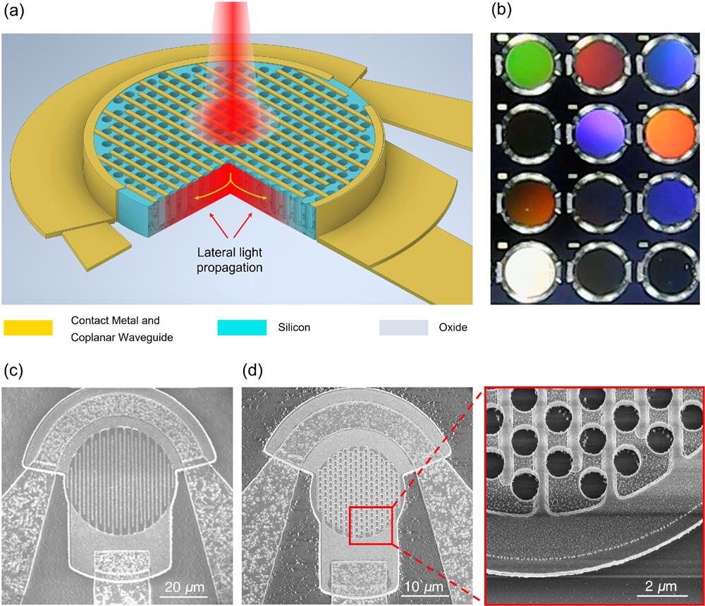
A thin Si slab with a thickness of integrated with a photon-trapping structure of cylindrical shape is designed to maximize light absorption. In this effort, the geometry is optimized for the lattice structure, diameter, period, and depth of the photon-trapping holes that are filled with air. The cross-sectional structure is schematically shown in Fig. 1(a) and Figs. S2 and S7 in the Supplementary Material. To fabricate the photodetectors, we have exploited the standard CMOS-compatible infrastructure. We have opted for a mesa-based photodetector geometry where the photon trapping holes are patterned on the top mesa. The devices are fabricated on a silicon-on-insulator (SOI) substrate with a thick active Si layer (the absorber layer). Figure 1(b) showcases the optical micrographs of the fabricated photodetectors for a range of hole diameter () and periodicity (). Detailed microscopic images of the fabricated device are shown in Fig. S3 in the Supplementary Material. A firsthand confirmation of the wavelength selectivity of these photon-trapping holes is evident from the different color spectra revealed during microscopic imaging for different devices with different and [Fig. 1(b)]. The scanning electron microscopy (SEM) images of the planar and photon-trapping photodetectors are shown in Figs. 1(c) and 1(d), respectively. The planar (without holes) photodetectors are used as a control device to benchmark the performance enhancement resulting from the hole-array introduction. The inset of Fig. 1(d) indicates that the patterned holes are circular. Interdigitated aluminum fingers with a thickness of 100 nm and width of 300 nm are sputtered on Si. Cylindrical photon-trapping holes with a , , and hole depth of 1300, 1000, and 600 nm, respectively, are etched in the Si active layer. Fabricated photodetectors are isolated from each other, and coplanar waveguides (CPWs) were delineated for high-speed operation. The roughness observed on the CPW pads and the presence of residual dielectric particles on the Si surface were a result of the hydrofluoric acid (HF) passivation process during fabrication. Despite these effects, the optical measurement remained unaffected. The details of the fabrication method are discussed in Fig. S1 in the Supplementary Material.47
![]()
Figure 1.Design and fabrication of highly absorbing thin-film Si photon-trapping photodetector. (a) Schematic of the photon-trapping silicon MSM photodetector. The photon-trapping cylindrical hole arrays allow lateral propagation by bending the incident light, resulting in an enhanced photon absorption in Si. (b) Optical microscopy images of the photon-trapping photodetectors fabricated on a
3 Leapfrogging the Absorption Coefficient of Thin Si beyond That of Intrinsic GaAs
Using the Bouguer–Beer–Lambert law and considering surface reflection losses,54,55 an effective absorption coefficient (), defined in Eq. (1), is estimated to quantify the enhancement in photon absorption of the fabricated devices with photon-trapping structures,
![]()
Figure 2.Experimental demonstration of absorption enhancement in Si that exceeds the intrinsic absorption limit of GaAs. (a) Comparison of the enhanced absorption coefficients (
Next, we study QE, an essential performance metric to quantify the optical sensitivity of the fabricated photodetectors. The measured QE of photon-trapping photodetectors for incident wavelengths ranging from 800 to 905 nm is shown in Fig. 2(b). We have shown a comparison of QEs of planar and photon-trapping photodetectors. External quantum efficiencies over 80% are observed experimentally in the photon-trapping photodetectors for incident wavelengths below 860 nm. Owing to Si’s inherent optical material properties, the absorption decreases sharply above 860 nm wavelength, with a minimum value as low as 68% at 905 nm. However, compared to the photodetectors with a planar surface, the absorption efficiency is increased by in photon-trapping photodetectors at 850 nm wavelength. The corresponding responsivities of the photon-trapping devices exhibit more than 500 mA/W, as shown in Fig. S11 in the Supplementary Material. In addition, the minimum enhancement of QE in all the fabricated photon-trapping photodetectors compared to the planar devices is at least more than 280% for the wavelength spectrum between 800 and 905 nm. The measured QEs also exhibit an excellent agreement with simulated QEs in both planar and photon-trapping devices, as depicted in Fig. 2(b). The detailed simulation study is discussed in the following section and in the Supplementary Material. Such a high-absorption enhancement directly results from the generation of optical modes propagating laterally due to the integrated photon-trapping surface structures (Video 2). Notably, such photon-trapping photodetectors exhibit reduced capacitance compared to their planar counterpart due to reduced surface areas caused by the photon-trapping structures, as experimentally characterized and depicted in Fig. 2(c), leading to enhance bandwidth in the device. Such reduction in capacitance can further strengthen the ultrafast response of the devices caused by the thin absorption layer. The corresponding dark current of the planar and the photon-trapping devices are also provided in Fig. S10 in the Supplementary Material. So far, to the best of our knowledge, such a high-photoabsorption enhancement in the Si photodetector is the first experimental demonstration.
4 Performance Prediction for Ultrathin Photon-Trapping Si Photodetectors
Leaping on the experimental demonstration of extraordinary enhancement in the performance of photon-trapping photodetectors fabricated on thin Si, optical simulations are performed by an FDTD method for the most optimized photon-trapping structure with a , , and depth of 1000, 700, and 600 nm, respectively. Again, it should be mentioned here that the best dimension for the fabricated devices was , , and . The discrepancy could occur due to the limitations of the fabrication technologies.51 The detail of the optical simulation method is provided in the Supplementary Material. Such a photon-trapping structure is simulated for absorption in the wavelengths ranging from 800 to 1100 nm, as presented in Fig. 3(a). Photon-trapping structures with different lattice patterns and microhole shapes/channels also demonstrate a high-absorbing phenomenon, as provided in Figs. S8 and S9 in the Supplementary Material. Figure S9 in the Supplementary Material further demonstrates that different photon-trapping holes with different shapes would impact light–matter interactions in photodetectors differently. Additionally, a Si slab with a thickness and a planar surface is also simulated as a reference. The red curve represents simulated absorption spectra of the photon-trapping structure for normally incident light. The photon-trapping structure exhibits distinctly higher absorption in comparison with the planar structure. For Si structure with photon-trapping holes and the normally incident light illumination, a maximum photon absorption exceeding 85% is achieved around the 850 nm wavelength. The photon-trapping structures facilitate absorption enhancement through guided lateral modes for a broad range of NIR wavelengths. Figures 3(b) and 3(c) represent the calculated Poynting vector in the photon-trapping Si slab with thickness on the and planes. These figures demonstrate how an ensemble of integrated holes induces a change in the direction of the propagating photons from vertical to lateral orientation in Si films. Laterally oriented Poynting vectors form vortex-like circulation patterns around the sidewalls of the cylindrical holes, resulting in guided light propagation parallel to the photodetector surface for a prolonged time and enabling absorption in Si with high efficiency. Notably, the guided lateral modes in the Si active layer are also facilitated by the front and the back air/Si and Si/oxide layer interfaces, where the oxide layer of the SOI acts as a back reflector. It should be explicitly mentioned here that the oxide layer significantly facilitates the high absorption of photons in the active layer.51 A movie demonstrating the side view of energy density distribution mapping of a normally incident light beam that bends almost at a right angle into laterally propagating modes of light along the plane of the Si absorber layer with photon-trapping holes is provided in Video 2. To summarize, the photon-trapping surface structures increase the optical path length, which improves the absorption efficiency within the structure with the aid of enhanced light–matter interactions.
![]()
Figure 3.Theoretical demonstration of enhanced absorption characteristics in ultrathin Si film integrated with photon-trapping structures. (a) Comparison of simulated absorption of photon-trapping [
To study and analyze the photon absorption limits of ultrathin Si films used in modern CMOS processes, we further explored the absorption efficiency of 30 and 100 nm ultrathin Si films integrated with and without photon-trapping structures, as depicted in Fig. 3(d). Similar to the Si film with 1000 nm thickness, photon-trapping ultrathin Si film exhibits dramatically higher absorption efficiency than the planar Si film. This also proves that such enhancement in absorption is a direct consequence of enhanced light–matter interaction, irrespective of the film thickness, as visualized by Video 3. More than 21% and 8% absorption efficiencies are observed at 850 nm illumination wavelength in Si with 100 and 30 nm absorption thickness, respectively. In contrast, the absorption efficiency is for such ultrathin planar Si, as depicted in Fig. 3(d). The estimated for 100 and 30 nm Si layers are 23,572 and , respectively, which are significantly higher than the intrinsic absorption limit of GaAs at 850 nm wavelength.
Intriguingly, we also observed that the enhanced absorption coefficient of our fabricated devices effectively exceeds the limit, as provided in Fig. S12 in the Supplementary Material, where is the refractive index of Si at the corresponding wavelengths. Nevertheless, we cannot claim that it exceeds the light-trapping geometrical limit of ,15,19 since a collimated laser beam was used for device illumination. In contrast, an isotropic and incoherent light source is commonly used in solar cell characterization. For the case of a collimated beam, the geometrical limit is adjusted by , where is the angle between the light source and a plane perpendicular to the surface.27 We further noticed that the absorption enhancement of our devices could reach a maximum up to limit at 850 nm of incident wavelength (Fig. S12 in the Supplementary Material). Further investigation correlating the illumination angle of the collimated beams and absorption enhancement will help us understand whether the light-trapping geometrical limit can be overcome.
5 Physics-Based Explanation for the Performance Enhancement
Based on the above observations, photon-trapping structures effectively supporting lateral modes and efficient coupling of light are essential for the optimum enhancement of absorption efficiency. The eigenmodes of the microhole array determine the propagation of photons in the lateral direction. The calculated band structures and allowable available eigenmodes with small holes (, , and thickness, ) and large holes (, , and thickness, ) are shown in Figs. 4(a) and 4(b) and Fig. S14 in the Supplementary Material for the lateral light propagation in a thin film with an array of holes with the period and hole size . The band structure is calculated using the standard technique that converts Maxwell’s equations from space into space by solving the number of wave vectors , where is an integer number. The eigenmodes in the array were calculated at wavelengths near 850 nm, whereas the ratio of hole diameter to period of the photon-trapping photodetectors is assumed to be to make it consistent with the fabricated devices. The number of eigenmodes for the hole-array structures increases with an increasing value of , where is larger than unity. Figures 4(a) and 4(b) illustrate the relationship between lateral wave vector and the incident wavelength for a hole size of 100 and 700 nm, respectively, under TE and TM polarizations. The solid curves represent the solutions for ΓX and ΓM directions, whereas the dots represent the areas between those directions, which are also provided in Fig. S14 in the Supplementary Material. First, a high-absorption characteristic can be observed under both TM and TE light incidences, as seen in the band diagram [Figs. 4(a) and 4(b)] and the comparative absorption curves provided in Fig. S15 in the Supplementary Material. It is noticeable that the larger holes pronounce curves with a smaller slope, which corresponds to a smaller group velocity. The next question is the coupling into the array. When significant lateral field components are generated in the cylindrical coordinates for a hole with a specific dimension, the solutions of the wave vectors using Bessel functions can be given as , , and , where is the wave vector for a given frequency in the vacuum, is the dielectric constant of Si, and is the propagation constant. When the solution to the Bessel function is , the lateral wave vectors are coupled with eigenmodes. The cross of the solution or with the eigenmodes pronounces the modes that propagate laterally and can be absorbed in the material. It should be noted that the Bessel function was solved for a single hole, and it is expected that a similar characteristic can be achieved for an array of holes. For the small holes, we have the solutions only for the finite number of the eigenmodes with , which corresponds to the guided modes in photonic crystals. Such structures exhibit sharp spikes in absorption, as shown in Fig. 4(e). However, a continuous solution can be found in the large holey structures for the wavelengths ranging from 800 to 1000 nm, leading to a distinctly higher light absorption than in small holes, as depicted in Fig. 4(e). Hence, the optimized larger holey structures exhibit a good coupling phenomenon due to the relationship between the vector and the eigenmodes.
![]()
Figure 4.Reduced group velocity in photon-trapping Si (slow light) and enhanced optical coupling to lateral modes contribute to enhanced photon absorption. Calculated band structure of Si film with (a) small holes (
In the next step, the influence of the size of the holes on the formation of lateral optical modes and the corresponding field distribution is studied. Coupling phenomena are only observed in the photon-trapping structures, as presented in Fig. S16 in the Supplementary Material. Low-coupling phenomena are observed for the devices with hole sizes smaller than half the wavelength, as shown in Fig. 4(c), where photons cannot efficiently couple within the absorber layer. However, for the hole size comparable with the incident wavelength, the light can couple into the holes and leak out through the sides of the hole, as illustrated in Fig. 4(d). The incident photons also reflect from the surface of photodetectors when the hole diameter is smaller than the incident wavelength, which is not the case for our most efficient fabricated devices. The hole diameters of our most optimized fabricated devices are comparable to the incident wavelength, similar to the one shown in Fig. 4(d). In photodetectors with larger holes, photons accumulate in the plane around the hole after coupling into laterally propagating modes and eventually getting absorbed there. Furthermore, the vertically illuminated light refracts at angle from the boundary conditions, increasing light absorption in the active layer. Finally, the oxide layer of the SOI wafer underneath the sensors further contributes to enhanced photon absorption by reflecting the photons in the direction of the device surface. The influence of coupling for smaller and bigger holes at different incident angles is also studied on the photon absorption, as provided in Fig. S5 in the Supplementary Material. Photodetectors with larger holes () exhibit noticeably higher light absorption, irrespective of incident angles, than devices with smaller holes. However, when illuminated with photons of longer wavelengths, a relatively higher photon absorption is obtained for the incident angle of 30 deg compared with 0 deg in both small and larger holes.
Slow light with reduced group velocity increases absorption efficiency due to the augmented light–matter interactions. The group velocity was calculated from the band diagram as under TE polarization modes, as presented in Fig. 4(f). The group velocity in bulk Si was calculated as , where is the light velocity and is the refractive index of Si at 850 nm. The normalized frequency of our experimental structures is between 1.3 and 1.6. Herein, the group velocity in most modes for the normalized frequency between 1.3 and 1.6 is significantly lower than the group velocity of light in bulk Si. The average group velocity for the modes was also calculated, as shown by the red line, indicating a conspicuously lower average group velocity of the photon trapping structures compared to that of Si without such surface structures. Light-trapping surface structures have been demonstrated to be capable of enabling enhanced optical DOS with light enhancement beyond the ray optic limit.58,59 Herein, the DOS was also calculated as an integral over the wave vector for a given frequency, , in which and are differential dimension and energy, respectively. For the 2D photonic crystals, DOS could be approximated as .27 The DOS of the photon-trapping photo detectors is found to be higher than that of the photodetectors with planar surfaces, as provided in Fig. S13(a) in the Supplementary Material. The photodetectors with micro-hole periods shorter than the incident wavelengths exhibit noticeably low DOS compared to the periods comparable to and slightly longer than the wavelengths. Our designed and fabricated photodetectors closely match with the shaded area on the right half of Fig. S13(a) in the Supplementary Material, exhibiting high DOS for frequencies higher than 1.0 (periods are comparable to or slightly longer than the incident wavelengths). Nevertheless, the region with high values of needs more Fourier components, and the maximum peaks of the DOS are not as pronounced as expected, while there is a constant increase of the optical mode density with . We conclude that observed absorption enhancement in Si is a combined effect of slow light with reduced group velocity, the enhanced photonic DOS, lateral propagation of a large number of optical modes, and efficient coupling of incident photons to the photon-trapping structures integrated on the Si surface. The cumulative impacts of the aforementioned processes help Si enhance light absorption by more than 20-fold and exceed the intrinsic absorption limit of GaAs.
We used a thin Si film with photon-trapping structures to demonstrate ultrafast time response characteristics of full-width at half-maximum (FWHM) and 16 ps deconvolved time response at 850 nm, as shown in Fig. S13(b) in the Supplementary Material. Such ultrafast time response coupled with broadband very high-absorption efficiency exhibited by ultrathin Si helps overcome the bandwidth-absorption trade-off faced by the ultrafast photodetector community. This work, thus, is very relevant to the design and fabrication of extremely fast and highly sensitive integrated photodetectors using modern CMOS foundry processes that currently use ultrathin Si of similar thickness.
6 Conclusions
We presented an experimental demonstration of photoabsorption enhancement by more than in Si that effectively exceeds the intrinsic absorption limit of GaAs for a broad wavelength spectrum between 800 and 905 nm. In our demonstration, we used photodetectors designed with a thin Si film integrated with an array of periodic photon-trapping structures that allow the generation of slow light with reduced group velocity, enhanced photon DOS, and, consequently, very high density of laterally propagating slow and stationary optical modes. This results in a more prolonged light–matter interaction time within the thin absorption region of the device. Intriguingly, simulated performances for ultrathin silicon photodetectors with even thinner absorption regions, such as 30 and 100 nm thin films, exhibit similarly enhanced photosensitivity. Additionally, Si photon-trapping structures help reduce photodetectors’ capacitance compared to their planar counterpart, enabling faster response. The fabrication process is CMOS-compatible and can contribute to integrated photodetectors with ultrafast responses for quantum computing, data communication systems, emerging biomedical imaging applications, biosensing, and autonomous vehicles.
Wayesh Qarony, a postdoctoral scholar at the University of California Berkeley in the EECS Department, works jointly with the LBNL. He focuses on nanophotonic design, fabrication, and characterization of optoelectronic, photonics, and quantum semiconductor devices. He received his PhD in applied physics and MSc in electrical engineering from Hong Kong Polytechnic University and Jacobs University Bremen, Germany, respectively. Before joining UC Berkeley & LBNL, he was a postdoctoral scholar at ECE UC Davis.
Ahmed S. Mayet received his MS in electrical and computer engineering from the University of California, Davis, in 2017 and PhD in electrical and computer engineering with emphasis in biophotonics and bioimaging from the University of California, Davis, in 2023. His research focused on developing ultra-fast and efficient optoelectronic devices for ultra-fast optical communication, biomedical imaging, and NIR imaging and sensing. He joined Taibah University, Saudi Arabia, in 2023, where he is currently an assistant professor.
Ekaterina Ponizovskaya Devine received the MS and PhD degrees from the Moscow Institute of Physics and Technology (State University), Moscow, Russia, in 1999. She was with the Ames Center, NASA, Mountain View, CA, United States, where she was involved in the optimization and physics-based models for prognostics and automation. She is currently with W&WSens Device, Inc., Los Altos, CA, United States, where she is focusing on photonics and photodetectors.
Soroush Ghandiparsi received the BSc degree in electrical engineering and the MSc degree in nanophotonic engineering from the School of Engineering Emerging Technology, Sharif University of Technology, Tehran, Iran, in 2009 and 2012, respectively. He received PhD in electrical engineering with emphasis in biophotonics and bioimaging from the University of California, Davis. Currently, his research is focused on developing a novel high-speed and efficient Silicon-based photodetector integrated with transimpedance amplifier (TIA)/equalizer analog circuits in the photonic BiCMOS platform.
Cesar Bartolo-Perez graduated from the University of California, Davis, with a PhD in electrical and computer engineering. His research focused on the development of single-photon avalanche photodetectors for lidar and biomedical applications. He is currently developing silicon photonic integrated systems for the same applications. He also holds an MSc from the National Institute of Astrophysics, Optics and Electronics, Mexico, and a BSc in technology from the National University Autonomous of Mexico.
Ahasan Ahamed is a second-year graduate student pursuing his PhD in the Electrical and Electronics Engineering Department at the University of California, Davis. He received a BSc degree from Bangladesh University of Engineering and Technology in 2018. He is currently working on spectral response engineering of photontrapping photodiodes paving towards spectrometer-on-a-chip. His research also include designing ultra-fast photodiodes and SPADs for hyperspectral imaging.
Amita Rawat received her BTech degree in electrical engineering from IIT Patna, India, and her PhD in microelectronics (logic device variability modeling and device fabrication) from the Department of Electrical Engineering IIT Bombay. She worked in IMEC Leuven, Belgium, on compact modeling of advance logic transistors. She is currently working as a postdoctoral fellow at University of California, Davis, on optoelectronic device modeling, simulation, and fabrication.
Hasina H. Mamtaz received the BS in environmental engineering in 1995, from Middle East Technical University, Ankara, Turkey, and MS degree in computer engineering from California State University at Long Beach. She worked for Gazillion Bits, Inc., San Jose, CA, and W&WSens Devices, Inc., Los Altos, CA. Currently, she is a program manager at UC Davis.
Toshishige Yamada received the BS and MS degrees in physics from the University of Tokyo, Japan, and the PhD in electrical engineering from Arizona State University. Following a postdoctoral fellow in applied physics at Stanford University, he joined the NASA Ames Research Center, and Santa Clara University, CA. He is currently an adjunct professor at the UC Santa Cruz and studies the theory and simulations of advanced semiconductor materials and devices.
Shih-Yuan Wang received a BS engineering physics in 1969, from UC Berkeley; and PhD in electrical engineering and computer sciences, in 1977 from UC Berkeley. At HP Labs, SY worked on multimode vertical cavity surface emitting lasers and high speed III-V photodiodes, both of which became successful products. He is currently with W&WSens Devices, Inc. Los Altos, CA, working on silicon photodiodes compatible with CMOS process for CMOS image sensors, optical interconnects, and lidar applications.
M. Saif Islam received a BSc degree in physics from Middle East Technical University, Ankara, in 1994, an MS degree in physics from Bilkent University, Ankara, in 1996, and the PhD in electrical engineering from UCLA, in 2001. He joined the University of California, Davis, in 2004, where he is currently a professor. He is a fellow of AAAS, Optica, SPIE, IEEE, and the National Academy of Inventors.
References
[7] A. Kirmani et al. First-photon imaging. Science., 343, 58-61(2014).
[8] G. Allen, T. Chan. Artificial Intelligence and National Security(2017).
[13] A. Dargys, J. Kundrotas. Handbook on Physical Properties of Ge, Si, GaAs and InP(1994).
[16] P. Y. Yu, M. Cardona. Fundamentals of Semiconductors(1999).
[53] R. Maurand et al. A CMOS silicon spin qubit. Nat. Commun., 7, 1-6(2016).
[55] A. Beer. Grundriss des photometrischen Calcüles(1854).
[57] E. D. Palik. Handbook of Optical Constants of Solids, 1, xvii-xviii(1985).

Set citation alerts for the article
Please enter your email address
© Copyright 2018-2021 | Chinese Laser Press. All Rights Reserved 沪ICP备15018463号-20