Fanlu Zhang, Zhicheng Su, Zhe Li, Yi Zhu, Nikita Gagrani, Ziyuan Li, Mark Lockrey, Li Li, Igor Aharonovich, Yuerui Lu, Hark Hoe Tan, Chennupati Jagadish, Lan Fu. High-speed multiwavelength InGaAs/InP quantum well nanowire array micro-LEDs for next generation optical communications[J]. Opto-Electronic Science, 2023, 2(5): 230003
Search by keywords or author
- Opto-Electronic Science
- Vol. 2, Issue 5, 230003 (2023)

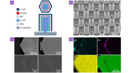
Fig. 1. (a ) Schematic of p-i-n InGaAs/InP single QW nanowire LED structure with lateral and vertical cross-sections. (b ) 30° tilted view SEM image of the nanowire array with a pitch of 800 nm. (c ) Cross-sectional STEM-HAADF image of a nanowire showing the hexagonal shape and radial QW under different magnifications. (d ) EDX elemental maps of the cross-sectional region in (c).

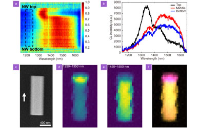
Fig. 2. (a ) SEM-CL spectral mapping of the InGaAs/InP single QW nanowire along the growth axis. The dashed rectangle indicates the relative position of the nanowire. (b ) CL spectrum is acquired from the nanowire’s top, middle, and bottom region, respectively. (c ) SEM image of the nanowire with the white arrow indicating nanowire growth direction. (d –e ) Spectrally integrated intensity map at 1250–1350 nm and 1450–1550 nm. (f ) Overlaid false-color CL image of (d–e), the pink and yellow region indicates the integrated CL intensity at 1250–1350 nm and 1450–1550 nm, corresponding to the emission from axial and radial QW, respectively.
Fig. 3. (a ) Schematic of fabricated nanowire array LED. (b ) L-I and I-V curves of a representative nanowire array LED. (c ) Voltage-dependent EL spectra at room temperature. (d ) Normalized voltage-dependent EL spectra from (c). (e ) Simulated voltage-dependent spontaneous emission spectra. (f ) Simulated emission spectrum at the bias of 1.2 V, with the decoupled contribution from axial and radial quantum wells.
Fig. 4. (a ) Average diameter of InGaAs/InP single QW nanowire from arrays with a pitch size of 0.8, 1.0 and 2.0 μm. (b ) Representative PL spectra measured from the top of the nanowire arrays with different pitch sizes. (c ) EL spectra measured at a forward bias of 1.5 V from nanowire array LED with different pitch sizes. (d ) Peak wavelength of the bias-dependent EL spectra from nanowire array LED with different pitch sizes.
Fig. 5. (a ) TRPL decay curve measured from the top of the nanowire array. (b ) TREL signal collected from pitch 0.8 µm nanowire array LED at modulation frequencies of 0.1, 0.6 and 1 GHz. (c ) 30° tilted SEM image of the nanowire arrays arranged corresponding to the letters “ANU”. (d ) Infrared camera image of the EL emission from nanowire array LEDs in (c) under various current injection levels.

Set citation alerts for the article
Please enter your email address


