• Infrared and Laser Engineering
  • Vol. 53, Issue 2, 20230567 (2024)
Sheng Ye1, Shangman Zhao1, Zhongfu Xing1、2, Zhiyong Peng2, Yuting Zheng1、3, Liangxian Chen1, Jinlong Liu1, Chengming Li1, and Junjun Wei1、3
Author Affiliations
  • 1Institute for Advanced Materials and Technology, University of Science and Technology, Beijing 100083, China
  • 2Tianjin Jinhang Institute of Technical Physics, Tianjin 300308, China
  • 3Shunde Graduate School, University of Science and Technology Beijing, Foshan 528399, China
  • show less
    DOI: 10.3788/IRLA20230567 Cite this Article
    Sheng Ye, Shangman Zhao, Zhongfu Xing, Zhiyong Peng, Yuting Zheng, Liangxian Chen, Jinlong Liu, Chengming Li, Junjun Wei. Research and application progress of laser technology in diamond processing[J]. Infrared and Laser Engineering, 2024, 53(2): 20230567 Copy Citation Text show less
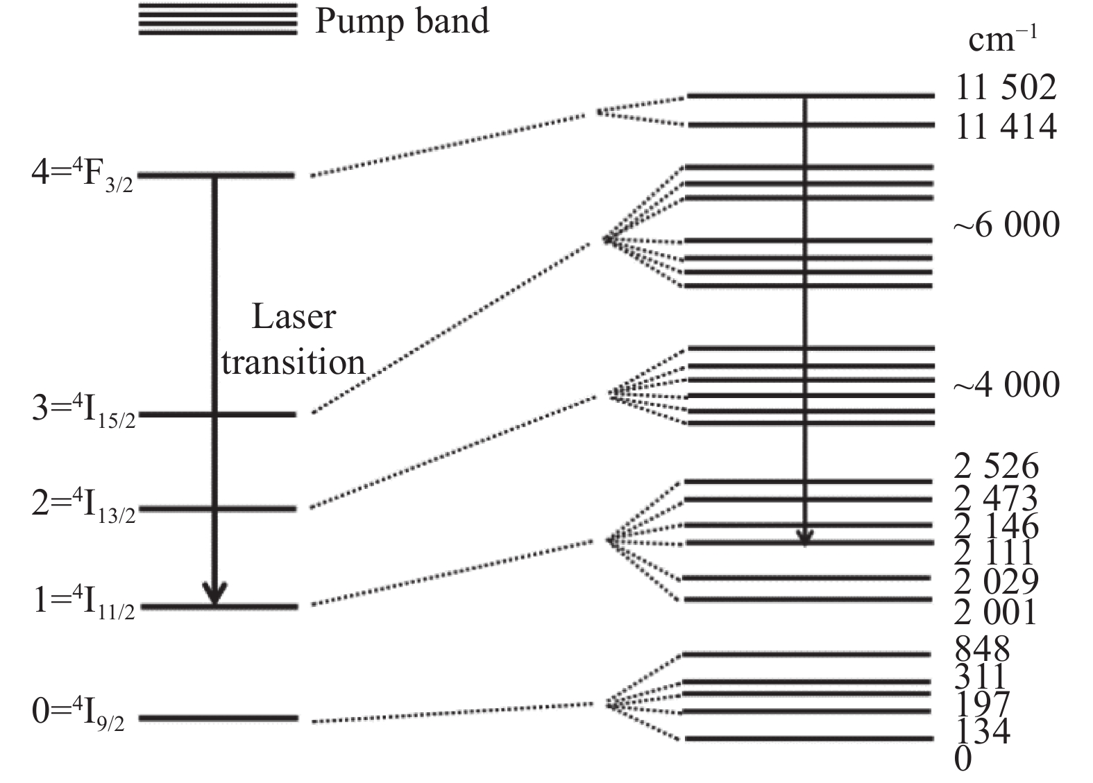
    Schematic diagram of energy level structure of Nd:YAG crystal[18]
    Fig. 1. Schematic diagram of energy level structure of Nd:YAG crystal[18]
    Absorption behavior of diamond and graphite [21]
    Fig. 2. Absorption behavior of diamond and graphite [21]
    Microscopic morphology of non-bond end-face grinding wheel with conical abrasive array structure[24]
    Fig. 3. Microscopic morphology of non-bond end-face grinding wheel with conical abrasive array structure[24]
    (a) Effect of pulse duration on diamond ablation threshold; (b) Incubation effect[25]
    Fig. 4. (a) Effect of pulse duration on diamond ablation threshold; (b) Incubation effect[25]
    Effect of plating different absorption layers on the transmittance of processed diamond [31]
    Fig. 5. Effect of plating different absorption layers on the transmittance of processed diamond [31]
    Fluorescence image of NV color center array[33]
    Fig. 6. Fluorescence image of NV color center array[33]
    Scanning electron microscope images of diamond surface irradiated by 800 nm femtosecond laser. (a) 170 nm periodic structure formed at 3000 pulse laser energy density of 1.9 J/cm2; (b) 190 nm periodic structure formed at 8000 pulse laser energy density of 2.8 J/cm2[36]
    Fig. 7. Scanning electron microscope images of diamond surface irradiated by 800 nm femtosecond laser. (a) 170 nm periodic structure formed at 3000 pulse laser energy density of 1.9 J/cm2; (b) 190 nm periodic structure formed at 8000 pulse laser energy density of 2.8 J/cm2[36]
    With the increase of pulse time delay, the evolution of diamond surface morphology array[37]
    Fig. 8. With the increase of pulse time delay, the evolution of diamond surface morphology array[37]
    Interaction model between laser, electron and lattice[23]. (a) Nanosecond laser; (b) Femtosecond laser
    Fig. 9. Interaction model between laser, electron and lattice[23]. (a) Nanosecond laser; (b) Femtosecond laser
    FIB cross sections of PCD composites obtained by: (a) Lapping; (b) Wire EDM; (c) Laser when pulse width =10 ps; (d) Laser when pulse width =125 ns; (e) Laser when pulse width =450 μs
    Fig. 10. FIB cross sections of PCD composites obtained by: (a) Lapping; (b) Wire EDM; (c) Laser when pulse width =10 ps; (d) Laser when pulse width =125 ns; (e) Laser when pulse width =450 μs
    Heat conduction and temperature distribution in the single crystal diamond at different scanning time, in which the arrowheads indicate the conductive heat flux direction[45]
    Fig. 11. Heat conduction and temperature distribution in the single crystal diamond at different scanning time, in which the arrowheads indicate the conductive heat flux direction[45]
    Raman spectral images of machined pits under different laser fluxes
    Fig. 12. Raman spectral images of machined pits under different laser fluxes
    Raman spectra of picosecond laser ablation of diamond micro-grooves at different laser energies
    Fig. 13. Raman spectra of picosecond laser ablation of diamond micro-grooves at different laser energies
    (a) Schematic diagram of ps laser processing; (b) Optical picture of graphitized microstructure device; (c) Influence of orientation on machining morphology and machining threshold[52-53]
    Fig. 14. (a) Schematic diagram of ps laser processing; (b) Optical picture of graphitized microstructure device; (c) Influence of orientation on machining morphology and machining threshold[52-53]
    Scanning electron microscope images of single crystal diamond surface processed by 200 fs laser. (a) Curved structure processed by laser pulse energy of 1.2 mJ; (b) The machined surface image when the laser pulse energy is 840 nJ; (c) An enlarged image of figure (b)[59]
    Fig. 15. Scanning electron microscope images of single crystal diamond surface processed by 200 fs laser. (a) Curved structure processed by laser pulse energy of 1.2 mJ; (b) The machined surface image when the laser pulse energy is 840 nJ; (c) An enlarged image of figure (b)[59]
    Surface morphology of laser processing. (a) Nanosecond laser; (b) Femtosecond lasers[60]
    Fig. 16. Surface morphology of laser processing. (a) Nanosecond laser; (b) Femtosecond lasers[60]
    Machining diamond through holes on silicon ball substrate by double pulse laser machining surface morpholog[68]
    Fig. 17. Machining diamond through holes on silicon ball substrate by double pulse laser machining surface morpholog[68]
    The average aspect ratio obtained in diamond is 40∶1[69]
    Fig. 18. The average aspect ratio obtained in diamond is 40∶1[69]
    Diamond microgrooves processed by process optimization parameters. (a) Surface morphology; (b) Cross-sectional morphology[26]
    Fig. 19. Diamond microgrooves processed by process optimization parameters. (a) Surface morphology; (b) Cross-sectional morphology[26]
    Photos of manifold diamond microchannel[75]
    Fig. 20. Photos of manifold diamond microchannel[75]
    Schematic diagram of laser ablation[79]
    Fig. 21. Schematic diagram of laser ablation[79]
    Surface roughness of diamond with different scanning ranges. (a) 100 μm×100 μm; (b)10 μm×10 μm[85]
    Fig. 22. Surface roughness of diamond with different scanning ranges. (a) 100 μm×100 μm; (b)10 μm×10 μm[85]
    The cross section SEM image of diamond sample after fs-laser treatment[87]
    Fig. 23. The cross section SEM image of diamond sample after fs-laser treatment[87]
    CO2 laser/water-guided laser hybrid machining system[88]
    Fig. 24. CO2 laser/water-guided laser hybrid machining system[88]
    Scanning electron microscope images of the ablation made with laser in silicon without. (a) And with water spray; (b) Both are made using 1000 pulses with 2.2 J energy per hole[93]
    Fig. 25. Scanning electron microscope images of the ablation made with laser in silicon without. (a) And with water spray; (b) Both are made using 1000 pulses with 2.2 J energy per hole[93]
    PropertyValueApplication
    Bandgap/eV5.4High-temperature electronics
    Carrier mobility/(cm2·V−1·s−1)Holes 3 800; electrons 4 500Radiation-hard detectors Optoelectronic switches
    Resistivity/Ω·cm1013-1015
    Thermal conductivity/(W·m−1·K−1)2 000-2 400Heat sinks
    Dielectric constant5.7
    Optical transmission range225 nm- radio frequencyPhotonics and MW devices
    Hardness/GPa(81±18)Tools, surgery blades
    Acoustic wave velocity/(km·s−1)18.4 along <100>Surface acoustic wave devices
    Thermal expansion coefficient/(10−6 ·K−1)0.8(293 K)Photonics and MW devices
    Corrosion resistanceStable in HFElectrochemistry
    Negative electron affinityElectron emitters
    BiocompatibilityBiomedicine
    Table 1. Properties and applications of diamond
    TypeNd:YAGTi:Al2O3CuAr+KrFArFCO2
    Wavelength/nm1 064532800510.548824819310 600
    Energy/eV1.172.331.552.422.545.06.420.12
    ModePulse/continuousPulsePulseContinuousPulsePulsePulse
    Table 2. Types of laser used in diamond processing
    Processing typeLaser typeHighlightProcessing resultReference
    Cutting193 nm;25 nsArgon gas is injected to change the processing atmosphereAvoid plasma heat damage[64]
    Cutting1.06 μm;100 μsThe optimum process parameters were determined by orthogonal experimentSection roughness: Ra=0.65 μm; Slit width: 173.1 μm; Taper: 5.9°[66]
    Drilling532 nm;20 nsLow taper, high aspect ratio structureMaximum aspect ratio: 66:1; Minimum taper: 0.1°(aspect ratio 10:1)[69]
    Drilling1030 nm;230 fsEffect of laser parameters on micropore geometryMicropore no debris, no heat damage[67]
    Microchannel800 nm;120 fsCombined with the experiment and simulation, the micro-channel "cold" machining is realizedInterface side taper <3°no residue, crack, edge breakage and other defects on the surface[26]
    Microchannel800 nm;100 fsThe diamond microstructure array constitutes the X-ray source array anodeMicrostructure groove width: 20 μm; Groove depth: 45 μm[74]
    Microchannel1060 nm;200 nsMicroslot linear repeat two scansThe bottom of the microgroove is wide and flat[42]
    Microchannel800 nm;120 fsLaser induced formation of nanoscale linear groovesSlot width: 40 nm; the groove depth is 500 nm;Length: 0.3 mm; Average spacing: (146±7) nm[78]
    Planarization355 nm;25 nsLaser polishing is directly used in optical device manufacturingRoughness Ra= 8.02 nm (20× 20 μm2); The light transmittance reaches 47.1%[79]
    Planarization1.06 μm;100 μsHigh efficiency flat rough diamond surfaceSurface roughness Sa= 1.9 μm; material removal rate 1.1mm3/min[9]
    Separation800 nm;50 fsThe laser forms a non-diamond phase on the subsurfaceElectrochemical stripping is achieved after epitaxial thickening[87]
    Hybrid laserCO2 laser/water guided laserThe CO2 laser is processed and the water guided laser is used to quench the heating zoneCut sheets faster[88]
    Water guided laser------The waterway extends the laser focus and improves the axial processing efficiencyWith a carbon layer formed only on the surface, stress is reduced[90]
    Water-assisted laser790 nm;120 fsWater mist assisted infrared laser ablationNo self-organizing structure is generated[93]
    Water-assisted laser532 nm;652 psCVD diamond-coated tools are used to process cross-scale microstructuresThe precise microslot array and two composite microstructures were prepared[96]
    Table 3. Research progress of different processing types of laser processing diamond
    Sheng Ye, Shangman Zhao, Zhongfu Xing, Zhiyong Peng, Yuting Zheng, Liangxian Chen, Jinlong Liu, Chengming Li, Junjun Wei. Research and application progress of laser technology in diamond processing[J]. Infrared and Laser Engineering, 2024, 53(2): 20230567
    Download Citation