
Tengteng Li, Qingyan Li, Xin Tang, Zhiliang Chen, Yifan Li, Hongliang Zhao, Silei Wang, Xin Ding, Yating Zhang, Jianquan Yao. Environment-friendly antisolvent tert-amyl alcohol modified hybrid perovskite photodetector with high responsivity[J]. Photonics Research, 2021, 9(5): 781
- Photonics Research
- Vol. 9, Issue 5, 781 (2021)
Abstract
1. INTRODUCTION
Photodetectors (PDs) that can convert hard-to-quantify optical signals into electrical ones that can be accurately detected are of great importance for a lot of industrial and scientific applications such as imaging, optical communications, chemical/biological sensing, and environmental monitoring [1–6]. For PDs, the most critical is the semiconductor material, which is used to absorb the incident photons and generate effective carriers (electrons and holes) upon photo-excitation. Then, the separated electrons and holes are transferred to the cathode and anode under the action of a built-in or applied electric field to produce an electric current [7]. At present, commercially available PDs mainly use inorganic semiconductor materials, such as GaN, Si, and InGaAs [8–11]. PDs using such materials have the advantages of a mature and reliable preparation process and a clear working mechanism, but the disadvantages are that the preparation process is complex and expensive [12], coupled with mechanical inflexibility and high driving voltage [13], which greatly limit their application scope. In the past few years, low-cost, solution-processable optoelectronic materials, such as organic materials, nanomaterials, and nanocomposites have shown great application potential in the preparation of flexible and large-area PDs [14–20], but shortcomings that cannot be ignored greatly hindered their broader applications and further development of the devices based on these materials, such as the low carrier mobility. Recently, perovskite materials have been widely used in solar cells [21–24], LEDs [25,26], lasers [27], and PDs [28,29] because of their unique characteristics, such as high carrier mobility, high optical absorption coefficient, long carrier diffusion length, and adjustable direct bandgap [30–32]. Perovskite PDs (PPDs) are suitable for visible light communication and imaging applications with a vertical structure because of the advantages of short carrier transmission distance, fast frequency response, and linear correlation between photocurrent and incident light intensity. Liu
In this work, tert-amyl alcohol (TAA) as a novel green antisolvent was first employed to prepare high-quality perovskite films with a smooth and mirror-like surface, which greatly improved the performance of the PPDs. Through this method, the responsivity of the PDs reached 1.56 A/W under the illumination of 532 nm laser with a power density of at a bias voltage of , which is a good responsivity we have known for PPDs with the vertical structure of glass/ITO/PEDOT:PSS/perovskite/PC61BM/BCP/Ag and only perovskite as the photosensitive material. The corresponding detectivity reached Jones, while the LDR reached 110 dB. In addition, we prepared PDs using isopropanol (IPA) and n-butanol (nBA) with polarity greater than TAA and toluene (TL) and chlorobenzene (CB) with polarity less than TAA as antisolvents for comparison. Judging from the obtained results, the PDs with TAA as the antisolvent had the best performance. We supposed that these results should be attributed to the better modification-assisted selectivity characteristics of TAA with moderate polarity than that of the other antisolvents, which would effectively regulate the formation of an intermediate phase staged in between a liquid precursor phase and a solid perovskite phase and further promote the homogeneous nucleation and crystal growth in the subsequent annealing process, thus leading to the formation of high-quality perovskite films and enhanced PD performance. Moreover, it is worth noting that TAA is a green and environment-friendly antisolvent material. Compared with TL, CB, and other high-risk antisolvents, it has the advantages of low toxicity, low cost, and easy availability. These results provide a reference for the preparation of high-performance and environment-friendly PPDs in the future.
2. EXPERIMENTAL SECTION
A. Materials Preparation
Poly(3,4-ethylenedioxythiophene):polystyrene sulfonate (PEDOT:PSS), lead iodide (, ), methylammonium iodide (, MAI, ), phenyl-C61-butyric acid methyl ester (, ), and bathocuproine (BCP, ) were all purchased from Xi’an Polymer Light Technology Corp., Ltd. N,N-dimethylformamide (DMF, 99.5%), dimethylsulfoxide (DMSO, 99.5%), and tert-amyl alcohol (TAA) were all purchased from Aladdin.
Sign up for Photonics Research TOC. Get the latest issue of Photonics Research delivered right to you!Sign up now
B. Device Fabrication
The prepatterned glass/ITO was first cleaned ultrasonically in the order of glass cleaner, deionized water, acetone, and isopropanol; then, the ITO glass was treated with UV-ozone for 15 min to enhance its wettability. The perovskite solution was prepared by dissolving and with a molar ratio of 1:1.05 in a mixed-solvent system with DMF and DMSO at a volume ratio of 9:1. A 100 μL perovskite precursor solution was spin-coated on the ITO/PEDOT:PSS substrate at 6000 r/min for 30 s, and 250 μL TAA was slowly dropped on the wet film at about one tenth of a second during the spin-coating process; then, the film was briefly annealed at 100°C for 15 s, while the film turned black. All the spin-coating processes mentioned above were carried out in a glove box filled with nitrogen. Next, the samples were annealed in ambient air at 100°C for 15 min and then annealed at DMSO atmosphere at 100°C for 10 min. Subsequently, the chlorobenzene solution of (20 mg/mL) and ethanol solution of BCP (0.7 mg/mL) were successively spin-coated on the perovskite film. Finally, 100 nm thick silver was evaporated as the electrode.
C. Characterization and Measurement
The cross-sectional images and surface morphologies of the different perovskite films were characterized using scanning electron microscopy (SEM, HITACHI SU 8020, Japan) and atomic force microscopy (AFM, CSPM5500, China). The cross-sectional EDS mapping images of different elements for each layer were characterized by a Talos F200X (FEI, America). The absorption of different antisolvent-processed perovskite films was measured by a Shimadzu UV-2600, Japan. The X-ray diffraction (XRD) measurement of perovskite films was performed by a D/MAX-2500, Japan. The steady-state and time-resolved photoluminescence spectra were recorded by a fluorescence spectrum (FLS 1000, Edinburgh Instruments, Britain). The Fourier transform infrared spectrum was recorded using the Nicolet iN10-FTIR microscope (Thermo Scientific, America). The I-V characteristics of all PDs under 405, 532, and 808 nm lasers illumination were measured using a Keithley 2400 source meter instrument.
3. RESULTS AND DISCUSSION
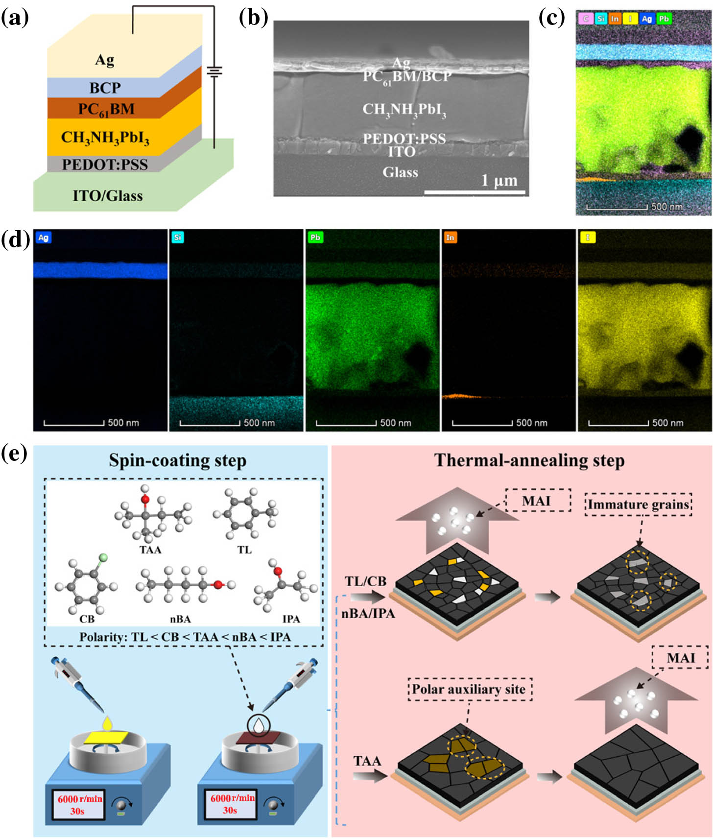
Figure 1.(a) Device architecture of PDs. (b) Cross-sectional SEM image of each layer in the device with a structure of (a). (c), (d) Cross-sectional EDS mapping images of different elements for each layer of the device in (a). (e) Schematic processing scheme of the antisolvent-assisted perovskite deposition process; the dashed parts are the chemical structures of antisolvents used in this work (TAA, TL, CB, nBA, and IPA).
![]()
Figure 2.(a) Photograph of TAA-PSK film on ITO glass before annealing. (b) FTIR spectra of TAA-PSK films with and without annealing. (c) Photographs of different antisolvents processed films after annealing.
![]()
Figure 3.Energy band and charge transfer diagram of PDs.
![]()
Figure 4.Optical properties of different antisolvent-processed films. (a) Absorption spectra. (b) XRD patterns. (c) Steady-state PL spectra; inset plots the corresponding emission peak position. (d) TRPL spectra; inset plots the values of
![]()
Figure 5.Morphologies of different antisolvents processed perovskite films. (a)–(e) Top-view SEM images; the scale bar is 1 μm. (f)–(j) AFM images; the scanned area is
![]()
Figure 6.Grain-size distribution histograms of films based on (a) TAA-PSK, (b) TL-PSK, (c) CB-PSK, (d) nBA-PSK, and (e) IPA-PSK measured by SEM images with the scale bar of 1 μm.
![]()
Figure 7.Electrical properties of PDs. (a)
Responsivity () as a crucial figure of merit to evaluate the performance of the PDs can be calculated by the equation [41] Performance Parameters of PPDs with Vertical StructureWavelength Responsivity Detectivity Response Time 500 0.87 [ 500 0.34 – [ 600 0.4 1.2 μs/3.2 μs [ 670 0.314 – 4 μs/3 μs [ 700 0.3 – – [ 660 0.18 – [ 532 1.56 204 ns/358 ns This work 532 0.46 320 ns/720 ns This work 532 0.61 304 ns/656 ns This work 532 0.35 348 ns/768 ns This work 532 0.30 364 ns/744 ns This work
![]()
Figure 8.Photoswitching properties of the PDs. (a) Photoswitching characteristics of the TAA-PD measured alternately in dark and under 532 nm laser illumination (
![]()
Figure 9.Electrical and photoswitching properties of TL-PD. (a)
![]()
Figure 10.Electrical and photoswitching properties of CB-PD. (a)
![]()
Figure 11.Electrical and photoswitching properties of nBA-PD. (a)
![]()
Figure 12.Electrical and photoswitching properties of IPA-PD. (a)
Meanwhile, as a control, we studied the photoswitching characteristics of the five PDs under the 532 nm laser illumination of at the bias of 0 V; the results are shown in Fig. 8(g). Compared with the other four comparison groups, TAA-PD has a more prominent photocurrent response under the same light conditions, indicating that TAA as an antisolvent to modify perovskite has great advantages compared with other antisolvents, which can effectively improve the quality of perovskite film and thus improve the photoelectric performance of the PD. In order to further understand the photoswitching characteristics of PDs, we also measured the photoresponse of the PDs under 405 and 808 nm laser illumination with a specific incident power density of and bias voltage of 0 V and compared the result with the photoresponse illuminated by 532 nm. As shown in Fig. 8(h), all PDs processed by different antisolvents have noticeable and fast photocurrent response under the illumination of three wavelengths of lasers. Remarkably, the photoswitching performance of TAA-PD under three wavelengths of illumination is significantly better than that of other comparison groups, further proving that the TAA is superior to TL, CB, nBA, and IPA in improving the performance of perovskite PDs; further, the histograms corresponding to the photocurrent response under three wavelengths of light irradiation given in Fig. 8(i)confirm this conclusion more intuitively. In addition, all PDs are more sensitive to the 532 nm laser, and the photocurrent response intensity to 405 and 808 nm light illumination decreases in turn, which is consistent with the absorption spectra in Fig. 4(a). Figure 8(j) displays the schematic diagram of the response time test system of the PDs. The pulse frequency of laser was controlled by a signal generator and was 100 kHz in this work. The pulse laser converged through lenses M1 and M2 and then illuminated to the perovskite PDs that connected to an oscilloscope with input resistance compensation after being restrained by an aperture diaphragm of proper size. The analog signals of response time were obtained by the oscilloscope monitoring.
4. CONCLUSIONS
In summary, we developed an effective solution-processed method for the fabrication of high-performance organometal trihalide PPDs. By introducing the novel and environment-friendly TAA as antisolvents for the first time, the responsivity of the PD reached 1.56 A/W under 532 nm laser illumination of , which is good responsivity for PPDs with the vertical structure of glass/ITO/PEDOT:PSS/MAPbI3/PC61BM/BCP/Ag. The superior performance of the TAA-PDcompared with other PDs in the comparison groups is mainly ascribed to the better modification-assisted selectivity characteristics of TAA with moderate polarity than those of the other antisolvents, which would effectively regulate the formation of an intermediate phase staged in between a liquid precursor phase and a solid perovskite phase and further promote the homogeneous nucleation and crystal growth in the subsequent annealing process, thus leading to the formation of high-quality perovskite films and enhanced PD performance. Moreover, compared with traditional antisolvents such as TL, CB, nBA, and IPA, TAA has less toxicity, which is more beneficial for management of the environment and health in the preparation process. Together, with the characteristics of low cost and easy availability, TAA is a great environment-friendly antisolvent with remarkable advantages for the fabrication of high-performance PPDs in the future and could provide a reference for similar research work.
References
[1] K. J. Baeg, M. Binda, D. Natali, M. Caironi, Y. Y. Noh. Organic light detectors: Photodiodes and phototransistors. Adv. Mater., 25, 4267-4295(2013).
[2] H. Chen, H. Liu, Z. Zhang, K. Hu, X. Fang. Nanostructured photodetectors: from ultraviolet to terahertz. Adv. Mater., 28, 403-433(2016).
[3] P. C. Eng, S. Song, B. Ping. State-of-the-art photodetectors for optoelectronic integration at telecommunication wavelength. Nanophotonics, 4, 277-302(2015).
[4] F. H. Koppens, T. Mueller, P. Avouris, A. C. Ferrari, M. S. Vitiello, M. Polini. Photodetectors based on graphene, other two-dimensional materials and hybrid systems. Nat. Nanotechnol., 9, 780-793(2014).
[5] J. Li, L. Niu, Z. Zheng, F. Yan. Photosensitive graphene transistors. Adv. Mater., 26, 5239-5273(2014).
[6] C. L. Tan, H. Mohseni. Emerging technologies for high performance infrared detectors. Nanophotonics, 7, 169-197(2018).
[7] L. Dou, Y. M. Yang, J. You, Z. Hong, W. H. Chang, G. Li, Y. Yang. Solution-processed hybrid perovskite photodetectors with high detectivity. Nat. Commun., 5, 5404(2014).
[8] H. J. Haugan, S. Elhamri, F. Szmulowicz, B. Ullrich, G. J. Brown, W. C. Mitchel. Study of residual background carriers in midinfrared InAs/GaSb superlattices for uncooled detector operation. Appl. Phys. Lett., 92, 071102(2008).
[9] M. Buscema, J. O. Island, D. J. Groenendijk, S. I. Blanter, G. A. Steele, H. S. van der Zant, A. Castellanos-Gomez. Photocurrent generation with two-dimensional van der Waals semiconductors. Chem. Soc. Rev., 44, 3691-3718(2015).
[10] A. Rogalski, J. Antoszewski, L. Faraone. Third-generation infrared photodetector arrays. J. Appl. Phys., 105, 091101(2009).
[11] F. P. García de Arquer, A. Armin, P. Meredith, E. H. Sargent. Solution-processed semiconductors for next-generation photodetectors. Nat. Rev. Mater., 2, 16100(2017).
[12] C. Xie, C. K. Liu, H. L. Loi, F. Yan. Perovskite-based phototransistors and hybrid photodetectors. Adv. Funct. Mater., 30, 1903907(2019).
[13] H. Wang, D. H. Kim. Perovskite-based photodetectors: materials and devices. Chem. Soc. Rev., 46, 5204-5236(2017).
[14] Y. Yao, Y. Liang, V. Shrotriya, S. Xiao, L. Yu, Y. Yang. Plastic near-infrared photodetectors utilizing low band gap polymer. Adv. Mater., 19, 3979-3983(2007).
[15] X. Zhou, D. Yang, D. Ma. Extremely low dark current, high responsivity, all-polymer photodetectors with spectral response from 300 nm to 1000 nm. Adv. Opt. Mater., 3, 1570-1576(2015).
[16] H. Y. Chen, M. K. Lo, G. Yang, H. G. Monbouquette, Y. Yang. Nanoparticle-assisted high photoconductive gain in composites of polymer and fullerene. Nat. Nanotechnol., 3, 543-547(2008).
[17] F. Guo, B. Yang, Y. Yuan, Z. Xiao, Q. Dong, Y. Bi, J. Huang. A nanocomposite ultraviolet photodetector based on interfacial trap-controlled charge injection. Nat. Nanotechnol., 7, 798-802(2012).
[18] G. Konstantatos, I. Howard, A. Fischer, S. Hoogland, J. Clifford, E. Klem, L. Levina, E. H. Sargent. Ultrasensitive solution-cast quantum dot photodetectors. Nature, 442, 180-183(2006).
[19] X. Gong, M. Tong, Y. Xia, W. Cai, J. S. Moon, Y. Cao, G. Yu, C. L. Shieh, B. Nilsson, A. J. Heeger. High-detectivity polymer photodetectors with spectral response from 300 nm to 1450 nm. Science, 325, 1665-1667(2009).
[20] V. Sukhovatkin, S. Hinds, L. Brzozowski, E. H. Sargent. Colloidal quantum-dot photodetectors exploiting multiexciton generation. Science, 324, 1542-1544(2009).
[21] D. Bi, C. Yi, J. Luo, J.-D. Décoppet, F. Zhang, S. M. Zakeeruddin, X. Li, A. Hagfeldt, M. Grätzel. Polymer-templated nucleation and crystal growth of perovskite films for solar cells with efficiency greater than 21%. Nat. Energy, 1, 16142(2016).
[22] Z. Yu, Z. Yang, Z. Ni, Y. Shao, B. Chen, Y. Lin, H. Wei, Z. J. Yu, Z. Holman, J. Huang. Simplified interconnection structure based on C60/SnO2-
[23] D. Zhao, Y. Yu, C. Wang, W. Liao, N. Shrestha, C. R. Grice, A. J. Cimaroli, L. Guan, R. J. Ellingson, K. Zhu, X. Zhao, R.-G. Xiong, Y. Yan. Low-bandgap mixed tin–lead iodide perovskite absorbers with long carrier lifetimes for all-perovskite tandem solar cells. Nat. Energy, 2, 17018(2017).
[24] N. Arora, M. I. Dar, A. Hinderhofer, N. Pellet, F. Schreiber, S. M. Zakeeruddin, M. Gratzel. Perovskite solar cells with CuSCN hole extraction layers yield stabilized efficiencies greater than 20%. Science, 358, 768-771(2017).
[25] T. H. Han, J. W. Lee, Y. J. Choi, C. Choi, S. Tan, S. J. Lee, Y. Zhao, Y. Huang, D. Kim, Y. Yang. Surface-2D/bulk-3D heterophased perovskite nanograins for long-term-stable light-emitting diodes. Adv. Mater., 32, 1905674(2020).
[26] Y. Shang, Y. Liao, Q. Wei, Z. Wang, B. Xiang, Y. Ke, W. Liu, Z. Ning. Highly stable hybrid perovskite light-emitting diodes based on Dion-Jacobson structure. Sci. Adv., 5, eaaw8072(2019).
[27] P. Liu, X. He, J. Ren, Q. Liao, J. Yao, H. Fu. Organic-inorganic hybrid perovskite nanowire laser arrays. ACS Nano, 11, 5766-5773(2017).
[28] X. Fu, S. Jiao, Y. Jiang, L. Li, X. Wang, C. Zhu, C. Ma, H. Zhao, Z. Xu, Y. Liu, W. Huang, W. Zheng, P. Fan, F. Jiang, D. Zhang, X. Zhu, X. Wang, A. Pan. Large-scale growth of ultrathin low-dimensional perovskite nanosheets for high-detectivity photodetectors. ACS Appl. Mater. Interfaces, 12, 2884-2891(2020).
[29] C. K. Liu, Q. Tai, N. Wang, G. Tang, H. L. Loi, F. Yan. Sn-based perovskite for highly sensitive photodetectors. Adv. Sci., 6, 1900751(2019).
[30] C. Zuo, H. J. Bolink, H. Han, J. Huang, D. Cahen, L. Ding. Advances in perovskite solar cells. Adv. Sci., 3, 1500324(2016).
[31] B. Saparov, D. B. Mitzi. Organic-inorganic perovskites: structural versatility for functional materials design. Chem. Rev., 116, 4558-4596(2016).
[32] Q. Chen, N. De Marco, Y. Yang, T.-B. Song, C.-C. Chen, H. Zhao, Z. Hong, H. Zhou, Y. Yang. Under the spotlight: the organic–inorganic hybrid halide perovskite for optoelectronic applications. Nano Today, 10, 355-396(2015).
[33] N. Ahn, D. Y. Son, I. H. Jang, S. M. Kang, M. Choi, N. G. Park. Highly reproducible perovskite solar cells with average efficiency of 18.3% and best efficiency of 19.7% fabricated via Lewis base adduct of lead(II) iodide. J. Am. Chem. Soc., 137, 8696-8699(2015).
[34] Y. Yun, F. Wang, H. Huang, Y. Fang, S. Liu, W. Huang, Z. Cheng, Y. Liu, Y. Cao, M. Gao, L. Zhu, L. Wang, T. Qin, W. Huang. A nontoxic bifunctional (anti)solvent as digestive-ripening agent for high-performance perovskite solar cells. Adv. Mater., 32, 1907123(2020).
[35] L. Wang, X. Wang, L.-L. Deng, S. Leng, X. Guo, C.-H. Tan, W. C. H. Choy, C.-C. Chen. The mechanism of universal green antisolvents for intermediate phase controlled high-efficiency formamidinium-based perovskite solar cells. Mater. Horiz., 7, 934-942(2020).
[36] H. Li, Y. Xia, C. Wang, G. Wang, Y. Chen, L. Guo, D. Luo, S. Wen. High-efficiency and stable perovskite solar cells prepared using chlorobenzene/acetonitrile antisolvent. ACS Appl. Mater. Interfaces, 11, 34989-34996(2019).
[37] F. Yang, G. Kapil, P. Zhang, Z. Hu, M. A. Kamarudin, T. Ma, S. Hayase. Dependence of acetate-based antisolvents for high humidity fabrication of CH3NH3PbI3 perovskite devices in ambient atmosphere. ACS Appl. Mater. Interfaces, 10, 16482-16489(2018).
[38] N. Sakai, S. Pathak, H.-W. Chen, A. A. Haghighirad, S. D. Stranks, T. Miyasaka, H. J. Snaith. The mechanism of toluene-assisted crystallization of organic–inorganic perovskites for highly efficient solar cells. J. Mater. Chem. A, 4, 4464-4471(2016).
[39] X. Xu, Z. Li, L. Zhu, H. Zheng, G. Liu, T. Hayat, A. Alsaedi, X. Zhang, Y. Huang, X. Pan. Large-grained formamidinium-based films via a 2D–3D conversion mechanism for high-performance perovskite solar cells without anti-solvent. J. Mater. Chem. A, 7, 1341-1348(2019).
[40] M. Yin, F. Xie, H. Chen, X. Yang, F. Ye, E. Bi, Y. Wu, M. Cai, L. Han. Annealing-free perovskite films by instant crystallization for efficient solar cells. J. Mater. Chem. A, 4, 8548-8553(2016).
[41] F. Li, C. Ma, H. Wang, W. Hu, W. Yu, A. D. Sheikh, T. Wu. Ambipolar solution-processed hybrid perovskite phototransistors. Nat. Commun., 6, 8238(2015).
[42] C. Liu, H. Peng, K. Wang, C. Wei, Z. Wang, X. Gong. PbS quantum dots-induced trap-assisted charge injection in perovskite photodetectors. Nano Energy, 30, 27-35(2016).
[43] C. Liu, K. Wang, C. Yi, X. Shi, P. Du, A. W. Smith, A. Karim, X. Gong. Ultrasensitive solution-processed perovskite hybrid photodetectors. J. Mater. Chem. C, 3, 6600-6606(2015).
[44] B. R. Sutherland, A. K. Johnston, A. H. Ip, J. Xu, V. Adinolfi, P. Kanjanaboos, E. H. Sargent. Sensitive, fast, and stable perovskite photodetectors exploiting interface engineering. ACS Photon., 2, 1117-1123(2015).
[45] C. Bao, W. Zhu, J. Yang, F. Li, S. Gu, Y. Wang, T. Yu, J. Zhu, Y. Zhou, Z. Zou. Highly flexible self-powered organolead trihalide perovskite photodetectors with gold nanowire networks as transparent electrodes. ACS Appl. Mater. Interfaces, 8, 23868-23875(2016).
[46] X. Zhang, C. Liu, G. Ren, S. Li, C. Bi, Q. Hao, H. Liu. High-switching-ratio photodetectors based on perovskite CH3NH3PbI3 nanowires. Nanomaterials, 8, 318(2018).
[47] H. Tao, H. Wang, Y. Bai, H. Zhao, Q. Fu, Z. Ma, H. Long. Efficient photodiode-type photodetectors with perovskite thin films derived from an MAPbI3 single-crystal precursor. J. Mater. Chem. C, 8, 6228-6235(2020).
[48] F. Yan, Z. Wei, X. Wei, Q. Lv, W. Zhu, K. Wang. Toward high-performance photodetectors based on 2D materials: strategy on methods. Small Methods, 2, 1700349(2018).
[49] Z.-Y. Peng, J.-L. Xu, J.-Y. Zhang, X. Gao, S.-D. Wang. Solution-processed high-performance hybrid photodetectors enhanced by perovskite/MoS2 bulk heterojunction. Adv. Mater. Interfaces, 5, 1800505(2018).
[50] C. Xie, C. Mak, X. Tao, F. Yan. Photodetectors based on two-dimensional layered materials beyond graphene. Adv. Funct. Mater., 27, 1603886(2017).

Set citation alerts for the article
Please enter your email address
© Copyright 2018-2021 | Chinese Laser Press. All Rights Reserved 沪ICP备15018463号-20