Journals >Review of Optics: a virtual journal


Halide perovskites, such as methylammonium lead halide perovskites (
Halide perovskites, such as methylammonium lead halide perovskites (
- Publication Date: Oct. 30, 2020
- Vol. 8 Issue 11 11000A56 (2020)


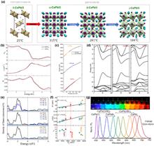
Two-dimensional (2D) perovskites are hybrid layered materials in which the inorganic lattice of an octahedron is sandwiched by organic layers. They behave as a quantum-well structure exhibiting large exciton binding energy and high emission efficiency, which is excellent for photonic applications. Hence, the cavity modulation and cavity devices of 2D perovskites are widely investigated. In this review, we summarize the rich photophysics, synthetic methods of different cavity structures, and the cavity-based applications of 2D perovskites. We highlight the strong exciton–photon coupling and photonic lasing obtained in different cavity structures. In addition, functional optoelectronic devices using cavity structures of 2D perovskites are also reviewed.
Two-dimensional (2D) perovskites are hybrid layered materials in which the inorganic lattice of an octahedron is sandwiched by organic layers. They behave as a quantum-well structure exhibiting large exciton binding energy and high emission efficiency, which is excellent for photonic applications. Hence, the cavity modulation and cavity devices of 2D perovskites are widely investigated. In this review, we summarize the rich photophysics, synthetic methods of different cavity structures, and the cavity-based applications of 2D perovskites. We highlight the strong exciton–photon coupling and photonic lasing obtained in different cavity structures. In addition, functional optoelectronic devices using cavity structures of 2D perovskites are also reviewed.
.- Publication Date: Oct. 30, 2020
- Vol. 8 Issue 11 11000A72 (2020)

The acceleration of polarized electrons, positrons, protons and ions in strong laser and plasma fields is a very attractive option for obtaining polarized beams in the multi-mega-electron volt range. Recently, there has been substantial progress in the understanding of the dominant mechanisms leading to high degrees of polarization, in the numerical modeling of these processes and in their experimental implementation. This review paper presents an overview on the current state of the field, and on the concepts of polarized laser–plasma accelerators and of beam polarimetry.
The acceleration of polarized electrons, positrons, protons and ions in strong laser and plasma fields is a very attractive option for obtaining polarized beams in the multi-mega-electron volt range. Recently, there has been substantial progress in the understanding of the dominant mechanisms leading to high degrees of polarization, in the numerical modeling of these processes and in their experimental implementation. This review paper presents an overview on the current state of the field, and on the concepts of polarized laser–plasma accelerators and of beam polarimetry.
.- Publication Date: Jan. 01, 1900
- Vol. 8 Issue 4 04000e36 (2020)
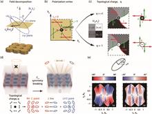
Manipulating radiation is important for a variety of optoelectronic applications, such as on-chip lasers, energy-efficient grating couplers, and antennas for light detection and ranging. Although designing and optimizing those optoelectronic devices are usually believed to be an engineering-oriented task, recent research reveals that the principles underlying radiation manipulation are closely connected to the concept of topology—the study of properties that are invariant under continuous deformations. In this review, we summarize a series of advances of the physics, phenomena, and applications related to radiation manipulation, in which topological concepts were adopted. Radiation could carry energy escaping from the system, breaking the energy conservation. The non-Hermiticity of such systems brings quite different physical consequences when comparing with the Hermitian counterparts and, hence, also results in the emergence of many interesting and extraordinary phenomena. In particular, it is found that the perfect trapping of light can still be realized in such non-Hermitian systems because of the photonic realization of bound states in the continuum. The fundamental nature of bound states in the continuum has been identified to be topological: they are essentially topological defects of the polarization vector field in momentum space, depicted by a kind of topological invariant named topological charges. Therefore, manipulation of radiation channels can be realized by controlling the topological charge evolution in momentum space. It is also demonstrated that the photonic states accompanied with different topological charges generate vortex beams with unique far-field radiation patterns, and ultra-fast switching of such vortex beams is demonstrated according to this principle. The progresses of topological photonics upon light radiation show that the topology is not just mathematical convenience for depicting photonic systems, but has brought realistic consequences in manipulating light and will boost the applications of photonics and optoelectronics in many aspects.
Manipulating radiation is important for a variety of optoelectronic applications, such as on-chip lasers, energy-efficient grating couplers, and antennas for light detection and ranging. Although designing and optimizing those optoelectronic devices are usually believed to be an engineering-oriented task, recent research reveals that the principles underlying radiation manipulation are closely connected to the concept of topology—the study of properties that are invariant under continuous deformations. In this review, we summarize a series of advances of the physics, phenomena, and applications related to radiation manipulation, in which topological concepts were adopted. Radiation could carry energy escaping from the system, breaking the energy conservation. The non-Hermiticity of such systems brings quite different physical consequences when comparing with the Hermitian counterparts and, hence, also results in the emergence of many interesting and extraordinary phenomena. In particular, it is found that the perfect trapping of light can still be realized in such non-Hermitian systems because of the photonic realization of bound states in the continuum. The fundamental nature of bound states in the continuum has been identified to be topological: they are essentially topological defects of the polarization vector field in momentum space, depicted by a kind of topological invariant named topological charges. Therefore, manipulation of radiation channels can be realized by controlling the topological charge evolution in momentum space. It is also demonstrated that the photonic states accompanied with different topological charges generate vortex beams with unique far-field radiation patterns, and ultra-fast switching of such vortex beams is demonstrated according to this principle. The progresses of topological photonics upon light radiation show that the topology is not just mathematical convenience for depicting photonic systems, but has brought realistic consequences in manipulating light and will boost the applications of photonics and optoelectronics in many aspects.
.- Publication Date: Oct. 21, 2020
- Vol. 8 Issue 11 11000B25 (2020)
- Publication Date: Dec. 10, 2020
- Vol. 18 Issue 12 121702 (2020)

- Publication Date: Nov. 10, 2020
- Vol. 18 Issue 11 110502 (2020)
- Publication Date: Oct. 22, 2020
- Vol. 8 Issue 11 11001703 (2020)
This paper presents a comprehensive review of recent advances in micro-additive manufacturing enabled by novel optical methods with an emphasis on photopolymerization-based printing processes. Additive manufacturing, also known as three-dimensional (3D) printing, has become an important engineering solution to construct customized components or functional devices at low cost. As a green manufacturing technology, 3D printing has the advantages of high energy efficiency, low material consumption, and high precision. The rapid advancement of 3D printing technology has broadened its applications from laboratory research to industrial manufacturing. Generally, 3D objects to be printed are constructed digitally [e.g., via computer-aided design (CAD) programs] by connecting a 3D dot array, where a dot is defined as a voxel through mechanical, electrical, or optical means. The voxel size ranges from a few orders of magnitude of the wavelength of light to the sub-diffraction limit, achieved by material nonlinearity and precise power thresholding. In recent years, extensive research in optical additive manufacturing has led to various breakthroughs in quality, rate, and reproducibility. In this paper, we review various micro-3D printing techniques, including single-photon and two-photon processes, with a focus on innovative optical methods, e.g., ultrafast beam shaping, digital holography, and temporal focusing. We also review and compare recent technological advances in serial and parallel scanning systems from the perspectives of resolution, rate, and repeatability, where the strengths and weaknesses of different methods are discussed for both fundamental and industrial applications.
This paper presents a comprehensive review of recent advances in micro-additive manufacturing enabled by novel optical methods with an emphasis on photopolymerization-based printing processes. Additive manufacturing, also known as three-dimensional (3D) printing, has become an important engineering solution to construct customized components or functional devices at low cost. As a green manufacturing technology, 3D printing has the advantages of high energy efficiency, low material consumption, and high precision. The rapid advancement of 3D printing technology has broadened its applications from laboratory research to industrial manufacturing. Generally, 3D objects to be printed are constructed digitally [e.g., via computer-aided design (CAD) programs] by connecting a 3D dot array, where a dot is defined as a voxel through mechanical, electrical, or optical means. The voxel size ranges from a few orders of magnitude of the wavelength of light to the sub-diffraction limit, achieved by material nonlinearity and precise power thresholding. In recent years, extensive research in optical additive manufacturing has led to various breakthroughs in quality, rate, and reproducibility. In this paper, we review various micro-3D printing techniques, including single-photon and two-photon processes, with a focus on innovative optical methods, e.g., ultrafast beam shaping, digital holography, and temporal focusing. We also review and compare recent technological advances in serial and parallel scanning systems from the perspectives of resolution, rate, and repeatability, where the strengths and weaknesses of different methods are discussed for both fundamental and industrial applications.
.- Publication Date: Nov. 12, 2020
- Vol. 8 Issue 12 12001827 (2020)
- Publication Date: Nov. 30, 2020
- Vol. 8 Issue 12 12001910 (2020)
- Publication Date: Sep. 21, 2020
- Vol. 2 Issue 5 054001 (2020)
- Publication Date: Oct. 30, 2020
- Vol. 2 Issue 5 054002 (2020)
- Publication Date: Nov. 04, 2020
- Vol. 2 Issue 6 064001 (2020)
- Publication Date: Dec. 07, 2021
- Vol. 3 Issue 6 064002 (2021)

About the Cover
Review of Optics: a virtual journal, started in 2019, is a virtual review journal, and it contains high-quality review articles from journals that published by Chinese Laser Press independently or along with its partners. Review of Optics is published quarterly. It aims to provide readers an alternative way to quickly look through high quality review papers. The scope of Review of Optics covers the full area of optics and photonics and relevant interdisciplinary topics, and meanwhile is in accordance with its source journals: Advanced Photonics, Chinese Optics Letters, High Power Laser Science and engineering and Photonics Research.