- Special Issue
- Next-generation Silicon Photonics
- 14 Article (s)

Next-generation silicon photonics: introduction
Daoxin Dai, Di Liang, and Pavel Cheben
In the past decade, silicon photonics has been making tremendous progress in terms of device functionality and performances as well as circuit integration for many practical applications ranging from communication, sensing, and information processing. This special issue, including four review articles and nine research articles, aims to provide a comprehensive overview of this exciting field. They offer a collective summary of recent progresses, in-depth discussions of the state-of-the-art, and insights into forthcoming developments that are well poised to drive silicon photonics technology into its next generation. In the past decade, silicon photonics has been making tremendous progress in terms of device functionality and performances as well as circuit integration for many practical applications ranging from communication, sensing, and information processing. This special issue, including four review articles and nine research articles, aims to provide a comprehensive overview of this exciting field. They offer a collective summary of recent progresses, in-depth discussions of the state-of-the-art, and insights into forthcoming developments that are well poised to drive silicon photonics technology into its next generation.
Photonics Research
- Publication Date: Sep. 29, 2022
- Vol. 10, Issue 10, NGSP1 (2022)


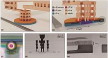
Miniature, highly sensitive MOSCAP ring modulators in co-optimized electronic-photonic CMOS
Hayk Gevorgyan, Anatol Khilo, Mark T. Wade, Vladimir M. Stojanović, and Miloš A. Popović
Convergence of high-performance silicon photonics and electronics, monolithically integrated in state-of-the-art CMOS platforms, is the holy grail for enabling the ultimate efficiencies, performance, and scaling of electronic-photonic systems-on-chip. It requires the emergence of platforms that combine state-of-the-art RF transistors with optimized silicon photonics, and a generation of photonic device technology with ultralow energies, increased operating spectrum, and the elimination of power-hungry thermal tuning. In this paper, in a co-optimized monolithic electronics-photonics platform (GlobalFoundries 45CLO), we turn the metal-oxide-semiconductor (MOS) field-effect transistor’s basic structure into a novel, highly efficient MOS capacitor ring modulator. It has the smallest ring cavity (1.5 μm radius), largest corresponding spur-free free spectral range (FSR=8.5 THz), and record 30 GHz/V shift efficiency in the O-band among silicon modulators demonstrated to date. With 1Vpp RF drive, we show an open optical eye while electro-optically tuning the modulator to track over 400 pm (69 GHz) change in the laser wavelength (using 2.5VDC range). A 90 GHz maximum electro-optic resonance shift is demonstrated with under 40 nW of power, providing a strong nonthermal tuning mechanism in a CMOS photonics platform. The modulator has a separately optimized body layer but shares the gate device layer and the gate oxide with 45 nm transistors, while meeting all CMOS manufacturability design rules. This type of convergent evolution of electronics and photonics may be the future of platforms for high-performance systems-on-chip. Convergence of high-performance silicon photonics and electronics, monolithically integrated in state-of-the-art CMOS platforms, is the holy grail for enabling the ultimate efficiencies, performance, and scaling of electronic-photonic systems-on-chip. It requires the emergence of platforms that combine state-of-the-art RF transistors with optimized silicon photonics, and a generation of photonic device technology with ultralow energies, increased operating spectrum, and the elimination of power-hungry thermal tuning. In this paper, in a co-optimized monolithic electronics-photonics platform (GlobalFoundries 45CLO), we turn the metal-oxide-semiconductor (MOS) field-effect transistor’s basic structure into a novel, highly efficient MOS capacitor ring modulator. It has the smallest ring cavity (1.5 μm radius), largest corresponding spur-free free spectral range (FSR=8.5 THz), and record 30 GHz/V shift efficiency in the O-band among silicon modulators demonstrated to date. With 1Vpp RF drive, we show an open optical eye while electro-optically tuning the modulator to track over 400 pm (69 GHz) change in the laser wavelength (using 2.5VDC range). A 90 GHz maximum electro-optic resonance shift is demonstrated with under 40 nW of power, providing a strong nonthermal tuning mechanism in a CMOS photonics platform. The modulator has a separately optimized body layer but shares the gate device layer and the gate oxide with 45 nm transistors, while meeting all CMOS manufacturability design rules. This type of convergent evolution of electronics and photonics may be the future of platforms for high-performance systems-on-chip.
Photonics Research
- Publication Date: Dec. 22, 2021
- Vol. 10, Issue 1, 010000A1 (2022)
Compact low-birefringence polarization beam splitter using vertical-dual-slot waveguides in silicon carbide integrated platforms
Xiaodong Shi, Jingjing Zhang, Weichen Fan, Yaoqin Lu, Nianhua Peng, Karsten Rottwitt, and Haiyan Ou
The polarization beam splitter is a key component for polarization manipulation in photonic integrated circuits, but it is challenging to design for low-refractive-index optical materials, due to the low birefringence of the waveguides. We propose what we believe is a novel compact vertical-dual-slot waveguide-based coupling scheme for silicon carbide, enabling efficient low-birefringence polarization splitting by extensively modulating the transverse-magnetic mode distribution. We numerically and experimentally demonstrate the device in the 4H-silicon-carbide-on-insulator integrated platform, with a small footprint of 2.2 μm×15 μm. The device, easy to fabricate via a single lithography process as other components on the chip, exhibits low insertion loss of <0.71 dB and <0.51 dB for the transverse-electric and transverse-magnetic polarized light, respectively, and polarization extinction ratio of >13 dB, over 80 nm wavelength range. The polarization beam splitter is a key component for polarization manipulation in photonic integrated circuits, but it is challenging to design for low-refractive-index optical materials, due to the low birefringence of the waveguides. We propose what we believe is a novel compact vertical-dual-slot waveguide-based coupling scheme for silicon carbide, enabling efficient low-birefringence polarization splitting by extensively modulating the transverse-magnetic mode distribution. We numerically and experimentally demonstrate the device in the 4H-silicon-carbide-on-insulator integrated platform, with a small footprint of 2.2 μm×15 μm. The device, easy to fabricate via a single lithography process as other components on the chip, exhibits low insertion loss of <0.71 dB and <0.51 dB for the transverse-electric and transverse-magnetic polarized light, respectively, and polarization extinction ratio of >13 dB, over 80 nm wavelength range.
Photonics Research
- Publication Date: Dec. 22, 2021
- Vol. 10, Issue 1, 010000A8 (2022)
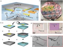
Wafer-level hermetically sealed silicon photonic MEMS
Gaehun Jo, Pierre Edinger, Simon J. Bleiker, Xiaojing Wang, Alain Yuji Takabayashi, Hamed Sattari, Niels Quack, Moises Jezzini, Jun Su Lee, Peter Verheyen, Iman Zand, Umar Khan, Wim Bogaerts, Göran Stemme, Kristinn B. Gylfason, and Frank Niklaus
The emerging fields of silicon (Si) photonic micro–electromechanical systems (MEMS) and optomechanics enable a wide range of novel high-performance photonic devices with ultra-low power consumption, such as integrated optical MEMS phase shifters, tunable couplers, switches, and optomechanical resonators. In contrast to conventional SiO2-clad Si photonics, photonic MEMS and optomechanics have suspended and movable parts that need to be protected from environmental influence and contamination during operation. Wafer-level hermetic sealing can be a cost-efficient solution, but Si photonic MEMS that are hermetically sealed inside cavities with optical and electrical feedthroughs have not been demonstrated to date, to our knowledge. Here, we demonstrate wafer-level vacuum sealing of Si photonic MEMS inside cavities with ultra-thin caps featuring optical and electrical feedthroughs that connect the photonic MEMS on the inside to optical grating couplers and electrical bond pads on the outside. We used Si photonic MEMS devices built on foundry wafers from the iSiPP50G Si photonics platform of IMEC, Belgium. Vacuum confinement inside the sealed cavities was confirmed by an observed increase of the cutoff frequency of the electro-mechanical response of the encapsulated photonic MEMS phase shifters, due to reduction of air damping. The sealing caps are extremely thin, have a small footprint, and are compatible with subsequent flip-chip bonding onto interposers or printed circuit boards. Thus, our approach for sealing of integrated Si photonic MEMS clears a significant hurdle for their application in high-performance Si photonic circuits. The emerging fields of silicon (Si) photonic micro–electromechanical systems (MEMS) and optomechanics enable a wide range of novel high-performance photonic devices with ultra-low power consumption, such as integrated optical MEMS phase shifters, tunable couplers, switches, and optomechanical resonators. In contrast to conventional SiO2-clad Si photonics, photonic MEMS and optomechanics have suspended and movable parts that need to be protected from environmental influence and contamination during operation. Wafer-level hermetic sealing can be a cost-efficient solution, but Si photonic MEMS that are hermetically sealed inside cavities with optical and electrical feedthroughs have not been demonstrated to date, to our knowledge. Here, we demonstrate wafer-level vacuum sealing of Si photonic MEMS inside cavities with ultra-thin caps featuring optical and electrical feedthroughs that connect the photonic MEMS on the inside to optical grating couplers and electrical bond pads on the outside. We used Si photonic MEMS devices built on foundry wafers from the iSiPP50G Si photonics platform of IMEC, Belgium. Vacuum confinement inside the sealed cavities was confirmed by an observed increase of the cutoff frequency of the electro-mechanical response of the encapsulated photonic MEMS phase shifters, due to reduction of air damping. The sealing caps are extremely thin, have a small footprint, and are compatible with subsequent flip-chip bonding onto interposers or printed circuit boards. Thus, our approach for sealing of integrated Si photonic MEMS clears a significant hurdle for their application in high-performance Si photonic circuits.
Photonics Research
- Publication Date: Jan. 14, 2022
- Vol. 10, Issue 2, 02000A14 (2022)
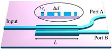
Ultra-power-efficient heterogeneous III–V/Si MOSCAP (de-)interleavers for DWDM optical links
Stanley Cheung, Geza Kurczveil, Yingtao Hu, Mingye Fu, Yuan Yuan, Di Liang, and Raymond G. Beausoleil
We discuss the design and demonstration of various III–V/Si asymmetric Mach–Zehnder interferometer (AMZI) and ring-assisted AMZI (de-)interleavers operating at O-band wavelengths with 65 GHz channel spacing. The wafer-bonded III–V/Si metal-oxide-semiconductor capacitor (MOSCAP) structure facilitates ultra-low-power phase tuning on a heterogeneous platform that allows for complete monolithic transceiver photonic integration. The second- and third-order MOSCAP AMZI (de-)interleavers exhibit cross-talk (XT) levels down to -22 dB and -32 dB with tuning powers of 83.0 nW and 53.0 nW, respectively. The one-, two-, and three-ring-assisted MOSCAP AMZI (de-)interleavers have XT levels down to -27 dB, -22 dB, and -20 dB for tuning powers of 10.0 nW, 7220.0 nW, and 33.6 nW, respectively. The leakage current density is measured to be in the range of 1.6–27 μA/cm2. To the best of our knowledge, we have demonstrated for the first time, athermal III–V/Si MOSCAP (de-)interleavers with the lowest XT and reconfiguration power consumption on a silicon platform. We discuss the design and demonstration of various III–V/Si asymmetric Mach–Zehnder interferometer (AMZI) and ring-assisted AMZI (de-)interleavers operating at O-band wavelengths with 65 GHz channel spacing. The wafer-bonded III–V/Si metal-oxide-semiconductor capacitor (MOSCAP) structure facilitates ultra-low-power phase tuning on a heterogeneous platform that allows for complete monolithic transceiver photonic integration. The second- and third-order MOSCAP AMZI (de-)interleavers exhibit cross-talk (XT) levels down to -22 dB and -32 dB with tuning powers of 83.0 nW and 53.0 nW, respectively. The one-, two-, and three-ring-assisted MOSCAP AMZI (de-)interleavers have XT levels down to -27 dB, -22 dB, and -20 dB for tuning powers of 10.0 nW, 7220.0 nW, and 33.6 nW, respectively. The leakage current density is measured to be in the range of 1.6–27 μA/cm2. To the best of our knowledge, we have demonstrated for the first time, athermal III–V/Si MOSCAP (de-)interleavers with the lowest XT and reconfiguration power consumption on a silicon platform.
Photonics Research
- Publication Date: Jan. 24, 2022
- Vol. 10, Issue 2, 02000A22 (2022)

High-speed silicon microring modulator at the 2 µm waveband with analysis and observation of optical bistability
Weihong Shen, Gangqiang Zhou, Jiangbing Du, Linjie Zhou, Ke Xu, and Zuyuan He
Recently, significantly raised interests have emerged for the 2 µm waveband as an extended new window for fiber optic communication. Much research progress has been made on the photonic integrated circuits for the 2 µm waveband, especially on the CMOS-compatible silicon-on-insulator wafer. In this work, a silicon integrated microring modulator (MRM) with record high-speed performances at the 2 µm waveband was demonstrated. An L-shaped PN junction was specially designed for 2 µm to achieve a high modulation efficiency with VπL of 0.85 V·cm. The measured 3 dB bandwidth is 18 GHz, supporting up to 50 Gbps signaling at 2 µm. Additionally, optical bistability induced by the thermo-optical effect and nonlinear effects was analyzed theoretically and observed experimentally in the 2 µm MRM for the first time to our knowledge. Nonlinear coupled mode theory and the Runge–Kutta method were used to simulate the behaviors of bistability in the 2 µm MRM. The simulation and experimental results indicate that, when the MRM is launched by a high optical power, the distorted resonant spectrum under an optical bistable state deteriorates the modulation efficiency and signal performances. This work breaks the record of high-speed silicon MRM at 2 µm, drawing a promising prospect for the silicon photonic integration and high-speed interconnection at the 2 µm waveband, and it provides the referenceable analysis of optical bistability, which guides the design and experimental investigation of 2 µm MRM. Recently, significantly raised interests have emerged for the 2 µm waveband as an extended new window for fiber optic communication. Much research progress has been made on the photonic integrated circuits for the 2 µm waveband, especially on the CMOS-compatible silicon-on-insulator wafer. In this work, a silicon integrated microring modulator (MRM) with record high-speed performances at the 2 µm waveband was demonstrated. An L-shaped PN junction was specially designed for 2 µm to achieve a high modulation efficiency with VπL of 0.85 V·cm. The measured 3 dB bandwidth is 18 GHz, supporting up to 50 Gbps signaling at 2 µm. Additionally, optical bistability induced by the thermo-optical effect and nonlinear effects was analyzed theoretically and observed experimentally in the 2 µm MRM for the first time to our knowledge. Nonlinear coupled mode theory and the Runge–Kutta method were used to simulate the behaviors of bistability in the 2 µm MRM. The simulation and experimental results indicate that, when the MRM is launched by a high optical power, the distorted resonant spectrum under an optical bistable state deteriorates the modulation efficiency and signal performances. This work breaks the record of high-speed silicon MRM at 2 µm, drawing a promising prospect for the silicon photonic integration and high-speed interconnection at the 2 µm waveband, and it provides the referenceable analysis of optical bistability, which guides the design and experimental investigation of 2 µm MRM.
Photonics Research
- Publication Date: Feb. 10, 2022
- Vol. 10, Issue 3, 03000A35 (2022)
Supercontinuum generation in silicon photonics platforms|Editors' Pick
Christian Lafforgue, Miguel Montesinos-Ballester, Thi-Thuy-Duong Dinh, Xavier Le Roux, Eric Cassan, Delphine Marris-Morini, Carlos Alonso-Ramos, and Laurent Vivien
Nonlinear optics has not stopped evolving, offering opportunities to develop novel functionalities in photonics. Supercontinuum generation, a nonlinear optical phenomenon responsible for extreme spectral broadening, attracts the interest of researchers due to its high potential in many applications, including sensing, imaging, or optical communications. In particular, with the emergence of silicon photonics, integrated supercontinuum sources in silicon platforms have seen tremendous progress during the past decades. This article aims at giving an overview of supercontinuum generation in three main silicon-compatible photonics platforms, namely, silicon, silicon germanium, and silicon nitride, as well as the essential theoretical elements to understand this fascinating phenomenon. Nonlinear optics has not stopped evolving, offering opportunities to develop novel functionalities in photonics. Supercontinuum generation, a nonlinear optical phenomenon responsible for extreme spectral broadening, attracts the interest of researchers due to its high potential in many applications, including sensing, imaging, or optical communications. In particular, with the emergence of silicon photonics, integrated supercontinuum sources in silicon platforms have seen tremendous progress during the past decades. This article aims at giving an overview of supercontinuum generation in three main silicon-compatible photonics platforms, namely, silicon, silicon germanium, and silicon nitride, as well as the essential theoretical elements to understand this fascinating phenomenon.
Photonics Research
- Publication Date: Mar. 01, 2022
- Vol. 10, Issue 3, 03000A43 (2022)
Polarization-independent multimode interference coupler with anisotropy-engineered bricked metamaterial
Carlos Pérez-Armenta, Alejandro Ortega-Moñux, José Manuel Luque-González, Robert Halir, Pedro J. Reyes-Iglesias, Jens Schmid, Pavel Cheben, Íñigo Molina-Fernández, and J. Gonzalo Wangüemert-Pérez
Many applications, including optical multiplexing, switching, and detection, call for low-cost and broadband photonic devices with polarization-independent operation. While the silicon-on-insulator platform is well positioned to fulfill most of these requirements, its strong birefringence hinders the development of polarization-agnostic devices. Here we leverage the recently proposed bricked metamaterial topology to design, for the first time, to our knowledge, a polarization-independent 2×2 multimode interference coupler using standard 220 nm silicon thickness. Our device can be fabricated with a single etch step and is optimized for the O-band, covering a wavelength range of 160 nm with excess loss, polarization-dependent loss, and imbalance below 1 dB and phase errors of less than 5°, as demonstrated with full three-dimensional finite-difference time-domain simulations. Many applications, including optical multiplexing, switching, and detection, call for low-cost and broadband photonic devices with polarization-independent operation. While the silicon-on-insulator platform is well positioned to fulfill most of these requirements, its strong birefringence hinders the development of polarization-agnostic devices. Here we leverage the recently proposed bricked metamaterial topology to design, for the first time, to our knowledge, a polarization-independent 2×2 multimode interference coupler using standard 220 nm silicon thickness. Our device can be fabricated with a single etch step and is optimized for the O-band, covering a wavelength range of 160 nm with excess loss, polarization-dependent loss, and imbalance below 1 dB and phase errors of less than 5°, as demonstrated with full three-dimensional finite-difference time-domain simulations.
Photonics Research
- Publication Date: Mar. 11, 2022
- Vol. 10, Issue 4, 04000A57 (2022)
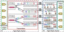
Achieving full grating-lobe-free field of view with low-complexity co-prime photonic beamforming transceivers
Aroutin Khachaturian, Reza Fatemi, and Ali Hajimiri
Integrated photonic active beamforming can significantly reduce the size and cost of coherent imagers for LiDAR and medical imaging applications. In current architectures, the complexity of photonic and electronic circuitry linearly increases with the desired imaging resolution. We propose a novel photonic transceiver architecture based on co-prime sampling techniques that breaks this trade-off and achieves the full (radiating-element-limited) field of view (FOV) for a 2D aperture with a single-frequency laser. Using only order-of-N radiating elements, this architecture achieves beamwidth and sidelobe level (SLL) performance equivalent to a transceiver with order-of-N2 elements with half-wavelength spacing. Furthermore, we incorporate a pulse amplitude modulation (PAM) row–column drive methodology to reduce the number of required electrical drivers for this architecture from order of N to order of N. A silicon photonics implementation of this architecture using two 64-element apertures, one for transmitting and one for receiving, requires only 34 PAM electrical drivers and achieves a transceiver SLL of -11.3 dB with 1026 total resolvable spots, and 0.6° beamwidth within a 23°×16.3° FOV. Integrated photonic active beamforming can significantly reduce the size and cost of coherent imagers for LiDAR and medical imaging applications. In current architectures, the complexity of photonic and electronic circuitry linearly increases with the desired imaging resolution. We propose a novel photonic transceiver architecture based on co-prime sampling techniques that breaks this trade-off and achieves the full (radiating-element-limited) field of view (FOV) for a 2D aperture with a single-frequency laser. Using only order-of-N radiating elements, this architecture achieves beamwidth and sidelobe level (SLL) performance equivalent to a transceiver with order-of-N2 elements with half-wavelength spacing. Furthermore, we incorporate a pulse amplitude modulation (PAM) row–column drive methodology to reduce the number of required electrical drivers for this architecture from order of N to order of N. A silicon photonics implementation of this architecture using two 64-element apertures, one for transmitting and one for receiving, requires only 34 PAM electrical drivers and achieves a transceiver SLL of -11.3 dB with 1026 total resolvable spots, and 0.6° beamwidth within a 23°×16.3° FOV.
Photonics Research
- Publication Date: Apr. 29, 2022
- Vol. 10, Issue 5, 05000A66 (2022)
Integrated scanning spectrometer with a tunable micro-ring resonator and an arrayed waveguide grating
Zunyue Zhang, Yi Wang, Jiarui Wang, Dan Yi, David Weng U Chan, Wu Yuan, and Hon Ki Tsang
Integrated spectrometers with both wide optical bandwidths and high spectral resolutions are required in applications such as spectral domain optical coherence tomography (SD-OCT). Here we propose a compact integrated scanning spectrometer by using a tunable micro-ring resonator (MRR) integrated with a single arrayed waveguide grating for operation in the 1265–1335-nm range. The spectral resolution of the spectrometer is determined by the quality factor of the MRR, and the optical bandwidth is defined by the free spectral range of the arrayed waveguide grating. The spectrometer is integrated with on-chip germanium photodetectors, which enable direct electrical readout. A 70-nm optical bandwidth and a 0.2-nm channel spacing enabled by scanning the MRR across one free spectral range are demonstrated, which offer a total of 350 wavelength channels with 31-kHz wavelength scanning speed. The integrated spectrometer is applied to measure different spectra and the interference signals from an SD-OCT system, which shows its great potential for future applications in sensing and imaging systems. Integrated spectrometers with both wide optical bandwidths and high spectral resolutions are required in applications such as spectral domain optical coherence tomography (SD-OCT). Here we propose a compact integrated scanning spectrometer by using a tunable micro-ring resonator (MRR) integrated with a single arrayed waveguide grating for operation in the 1265–1335-nm range. The spectral resolution of the spectrometer is determined by the quality factor of the MRR, and the optical bandwidth is defined by the free spectral range of the arrayed waveguide grating. The spectrometer is integrated with on-chip germanium photodetectors, which enable direct electrical readout. A 70-nm optical bandwidth and a 0.2-nm channel spacing enabled by scanning the MRR across one free spectral range are demonstrated, which offer a total of 350 wavelength channels with 31-kHz wavelength scanning speed. The integrated spectrometer is applied to measure different spectra and the interference signals from an SD-OCT system, which shows its great potential for future applications in sensing and imaging systems.
Photonics Research
- Publication Date: Apr. 29, 2022
- Vol. 10, Issue 5, 05000A74 (2022)
Guest Editors:
Daoxin Dai,
Zhejiang University, China (Lead Editor)
Di Liang,
Hewlett Packard Enterprise, USA
Pavel Cheben,
National Research Council of Canada, Canada
On the Cover of the virtual issue
© Copyright 2018-2021 | Chinese Laser Press. All Rights Reserved 沪ICP备15018463号-20