Journals > > Topics > Optoelectronics
Optoelectronics|88 Article(s)

Target-adaptive optical phased array lidar
Yunhao Fu, Baisong Chen, Wenqiang Yue, Min Tao, Haoyang Zhao, Yingzhi Li, Xuetong Li, Huan Qu, Xueyan Li, Xiaolong Hu, and Junfeng Song
Lidar based on the optical phased array (OPA) and frequency-modulated continuous wave (FMCW) technology stands out in automotive applications due to its all-solid-state design, high reliability, and remarkable resistance to interference. However, while FMCW coherent detection enhances the interference resistance capabilities, it concurrently results in a significant increase in depth computation, becoming a primary constraint for improving point cloud density in such perception systems. To address this challenge, this study introduces a lidar solution leveraging the flexible scanning characteristics of OPA. The proposed system categorizes target types within the scene based on RGB images. Subsequently, it performs scans with varying angular resolutions depending on the importance of the targets. Experimental results demonstrate that, compared to traditional scanning methods, the target-adaptive method based on semantic segmentation reduces the number of points to about one-quarter while maintaining the resolution of the primary target area. Conversely, with a similar number of points, the proposed approach increases the point cloud density of the primary target area by about four times. Lidar based on the optical phased array (OPA) and frequency-modulated continuous wave (FMCW) technology stands out in automotive applications due to its all-solid-state design, high reliability, and remarkable resistance to interference. However, while FMCW coherent detection enhances the interference resistance capabilities, it concurrently results in a significant increase in depth computation, becoming a primary constraint for improving point cloud density in such perception systems. To address this challenge, this study introduces a lidar solution leveraging the flexible scanning characteristics of OPA. The proposed system categorizes target types within the scene based on RGB images. Subsequently, it performs scans with varying angular resolutions depending on the importance of the targets. Experimental results demonstrate that, compared to traditional scanning methods, the target-adaptive method based on semantic segmentation reduces the number of points to about one-quarter while maintaining the resolution of the primary target area. Conversely, with a similar number of points, the proposed approach increases the point cloud density of the primary target area by about four times.
Photonics Research
- Publication Date: Apr. 12, 2024
- Vol. 12, Issue 5, 904 (2024)


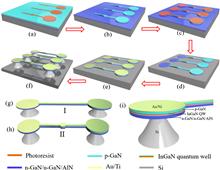
Electrically pumped optomechanical beam GaN-LED accelerometer based on the quantum-confined Stark effect
Gangyi Zhu, Xin Ji, Zhenfu Zhang, Xingcan Yan, Ying Yang, Feifei Qin, Xin Li, Jiagui Wu, Xiaojuan Sun, Junbo Yang, and Yongjin Wang
Micro-nano optomechanical accelerometers are widely used in automobile, aerospace, and other industrial applications. Here, we fabricate mechanical sensing components based on an electrically pumped GaN light-emitting diode (LED) with a beam structure. The relationship between the blueshift of the electroluminescence (EL) spectra and the deformation of the GaN beam structure based on the quantum-confined Stark effect (QCSE) of the InGaN quantum well (QW) structure is studied by introducing an extra mass block. Under the equivalent acceleration condition, in addition to the elastic deformation of GaN-LED, a direct relationship exists between the LED’s spectral shift and the acceleration’s magnitude. The extra mass block (gravitational force: 7.55×10⁻¹¹ N) induced blueshift of the EL spectra is obtained and shows driven current dependency. A polymer sphere (PS; gravitational force: 3.427×10⁻¹² N) is placed at the center of the beam GaN-LED, and a blueshift of 0.061 nm is observed in the EL spectrum under the injection current of 0.5 mA. The maximum sensitivity of the acceleration is measured to be 0.02 m/s2, and the maximum measurable acceleration is calculated to be 1.8×10⁶ m/s2. It indicates the simultaneous realization of high sensitivity and a broad acceleration measurement range. This work is significant for several applications, including light force measurement and inertial navigation systems with high integration ability. Micro-nano optomechanical accelerometers are widely used in automobile, aerospace, and other industrial applications. Here, we fabricate mechanical sensing components based on an electrically pumped GaN light-emitting diode (LED) with a beam structure. The relationship between the blueshift of the electroluminescence (EL) spectra and the deformation of the GaN beam structure based on the quantum-confined Stark effect (QCSE) of the InGaN quantum well (QW) structure is studied by introducing an extra mass block. Under the equivalent acceleration condition, in addition to the elastic deformation of GaN-LED, a direct relationship exists between the LED’s spectral shift and the acceleration’s magnitude. The extra mass block (gravitational force: 7.55×10⁻¹¹ N) induced blueshift of the EL spectra is obtained and shows driven current dependency. A polymer sphere (PS; gravitational force: 3.427×10⁻¹² N) is placed at the center of the beam GaN-LED, and a blueshift of 0.061 nm is observed in the EL spectrum under the injection current of 0.5 mA. The maximum sensitivity of the acceleration is measured to be 0.02 m/s2, and the maximum measurable acceleration is calculated to be 1.8×10⁶ m/s2. It indicates the simultaneous realization of high sensitivity and a broad acceleration measurement range. This work is significant for several applications, including light force measurement and inertial navigation systems with high integration ability.
Photonics Research
- Publication Date: Aug. 28, 2023
- Vol. 11, Issue 9, 1583 (2023)
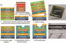
High-responsivity InAs quantum well photo-FET integrated on Si substrates for extended-range short-wave infrared photodetector applications|Editors' Pick
DaeHwan Ahn, Sunghan Jeon, Hoyoung Suh, Seungwan Woo, Rafael Jumar Chu, Daehwan Jung, Won Jun Choi, Donghee Park, Jin-Dong Song, Woo-Young Choi, and Jae-Hoon Han
Low-intensity light detection necessitates high-responsivity photodetectors. To achieve this, we report In0.53Ga0.47As/InAs/In0.53Ga0.47As quantum well (InAs QW) photo-field-effect-transistors (photo-FETs) integrated on a Si substrate using direct wafer bonding. Structure of the InAs QW channel was carefully designed to achieve higher effective mobility and a narrower bandgap compared with a bulk In0.53Ga0.47As, while suppressing the generation of defects due to lattice relaxations. High-performance 2.6 nm InAs QW photo-FETs were successfully demonstrated with a high on/off ratio of 105 and a high effective mobility of 2370 cm2/(V·s). The outstanding transport characteristics in the InAs QW channel result in an optical responsivity 1.8 times greater than InGaAs photo-FETs and the fast rising/falling times. Further, we experimentally confirmed that the InAs QW photo-FET can detect light in the short-wavelength infrared (SWIR; 1.0–2.5 μm) near 2 μm thanks to bandgap engineering through InAs QW structures. Our result suggests that the InAs QW photo-FET is promising for high-responsivity and extended-range SWIR photodetector applications. Low-intensity light detection necessitates high-responsivity photodetectors. To achieve this, we report In0.53Ga0.47As/InAs/In0.53Ga0.47As quantum well (InAs QW) photo-field-effect-transistors (photo-FETs) integrated on a Si substrate using direct wafer bonding. Structure of the InAs QW channel was carefully designed to achieve higher effective mobility and a narrower bandgap compared with a bulk In0.53Ga0.47As, while suppressing the generation of defects due to lattice relaxations. High-performance 2.6 nm InAs QW photo-FETs were successfully demonstrated with a high on/off ratio of 105 and a high effective mobility of 2370 cm2/(V·s). The outstanding transport characteristics in the InAs QW channel result in an optical responsivity 1.8 times greater than InGaAs photo-FETs and the fast rising/falling times. Further, we experimentally confirmed that the InAs QW photo-FET can detect light in the short-wavelength infrared (SWIR; 1.0–2.5 μm) near 2 μm thanks to bandgap engineering through InAs QW structures. Our result suggests that the InAs QW photo-FET is promising for high-responsivity and extended-range SWIR photodetector applications.
Photonics Research
- Publication Date: Aug. 01, 2023
- Vol. 11, Issue 8, 1465 (2023)

AlGaN solar-blind phototransistor capable of directly detecting sub-fW signals: self-depletion and photorecovery of full-channel 2DEG enabled by a quasi-pseudomorphic structure
Jiabing Lu, Zesheng Lv, and Hao Jiang
Heterojunction field-effect phototransistors using two-dimensional electron gas (2DEG) for carrier transport have great potential in photodetection owing to its large internal gain. A vital factor in this device architecture is the depletion and recovery of the 2DEG under darkness and illumination. This is usually achieved by adding an external gate, which not only increases the complexity of the fabrication and the electrical connection but also has difficulty ensuring low dark current (Idark). Herein, a quasi-pseudomorphic AlGaN heterostructure is proposed to realize the self-depletion and photorecovery of the 2DEG, in which both the barrier and the channel layers are compressively strained, making the piezoelectric and spontaneous polarization reverse, thus depleting the 2DEG and tilting the entire barrier and channel band to form two built-in photogates. The fabricated solar-blind phototransistors exhibit a very low Idark below 7.1×10⁻¹⁰ mA/mm, a superhigh responsivity (R) of 2.9×10⁹ A/W, a record high detectivity (D*) of 4.5×10²¹ Jones, and an ultrafast response speed at the nanosecond level. The high performance is attributed to the efficient depletion and recovery of the full 2DEG channel by the two photogates, enabling direct detection of the sub-fW signal. This work provides a simple, effective, and easily integrated architecture for carrier control and supersensitive photodetection based on polarization semiconductors. Heterojunction field-effect phototransistors using two-dimensional electron gas (2DEG) for carrier transport have great potential in photodetection owing to its large internal gain. A vital factor in this device architecture is the depletion and recovery of the 2DEG under darkness and illumination. This is usually achieved by adding an external gate, which not only increases the complexity of the fabrication and the electrical connection but also has difficulty ensuring low dark current (Idark). Herein, a quasi-pseudomorphic AlGaN heterostructure is proposed to realize the self-depletion and photorecovery of the 2DEG, in which both the barrier and the channel layers are compressively strained, making the piezoelectric and spontaneous polarization reverse, thus depleting the 2DEG and tilting the entire barrier and channel band to form two built-in photogates. The fabricated solar-blind phototransistors exhibit a very low Idark below 7.1×10⁻¹⁰ mA/mm, a superhigh responsivity (R) of 2.9×10⁹ A/W, a record high detectivity (D*) of 4.5×10²¹ Jones, and an ultrafast response speed at the nanosecond level. The high performance is attributed to the efficient depletion and recovery of the full 2DEG channel by the two photogates, enabling direct detection of the sub-fW signal. This work provides a simple, effective, and easily integrated architecture for carrier control and supersensitive photodetection based on polarization semiconductors.
Photonics Research
- Publication Date: Jun. 19, 2023
- Vol. 11, Issue 7, 1217 (2023)
All-in-one photoelectric logic gates by Dember photodetectors
Guoyang Cao, Changlei Wang, Yu Luo, and Xiaofeng Li
Photoelectric logic gates (PELGs) are the key component in integrated electronics due to their abilities of signal conversion and logic operations. However, traditional PELGs with fixed architectures can realize only very limited logic functions with relatively low on–off ratios. We present a self-driving polarized photodetector driven by the Dember effect, which yields ambipolar photocurrents through photonic modulation by a nested grating. The ambipolar response is realized by exciting the whispering-gallery mode and localized surface plasmon resonances, which leads to reverse spatial carrier generation and therefore the contrary photocurrent assisted by the Dember effect. We further design a full-functional PELG, which enables all five basic logic functions (“AND”, “OR”, “NOT”, “NAND”, and “NOR”) simultaneously in a single device by using one source and one photodetector only. Such an all-in-one PELG exhibits a strong robustness against structure size, incident wavelength, light power, and half-wave plate modulation, paving a way to the realization of ultracompact high-performance PELGs. Photoelectric logic gates (PELGs) are the key component in integrated electronics due to their abilities of signal conversion and logic operations. However, traditional PELGs with fixed architectures can realize only very limited logic functions with relatively low on–off ratios. We present a self-driving polarized photodetector driven by the Dember effect, which yields ambipolar photocurrents through photonic modulation by a nested grating. The ambipolar response is realized by exciting the whispering-gallery mode and localized surface plasmon resonances, which leads to reverse spatial carrier generation and therefore the contrary photocurrent assisted by the Dember effect. We further design a full-functional PELG, which enables all five basic logic functions (“AND”, “OR”, “NOT”, “NAND”, and “NOR”) simultaneously in a single device by using one source and one photodetector only. Such an all-in-one PELG exhibits a strong robustness against structure size, incident wavelength, light power, and half-wave plate modulation, paving a way to the realization of ultracompact high-performance PELGs.
Photonics Research
- Publication Date: Jun. 12, 2023
- Vol. 11, Issue 7, 1148 (2023)

Review on metal halide perovskite-based optoelectronic synapses
Xitong Hong, Xingqiang Liu, Lei Liao, and Xuming Zou
With the progress of both photonics and electronics, optoelectronic synapses are considered potential candidates to challenge the von Neumann bottleneck and the field of visual bionics in the era of big data. They are also regarded as the basis for integrated artificial neural networks (ANNs) owing to their flexible optoelectronic tunable properties such as high bandwidth, low power consumption, and high-density integration. Over the recent years, following the emergence of metal halide perovskite (MHP) materials possessing fascinating optoelectronic properties, novel MHP-based optoelectronic synaptic devices have been exploited for numerous applications ranging from artificial vision systems (AVSs) to neuromorphic computing. Herein, we briefly review the application prospects and current status of MHP-based optoelectronic synapses, discuss the basic synaptic behaviors capable of being implemented, and assess their feasibility to mimic biological synapses. Then, we focus on the two-terminal optoelectronic synaptic memristors and three-terminal transistor synaptic phototransistors (SPTs), the two essential apparatus structures for optoelectronic synapses, expounding their basic features and operating mechanisms. Finally, we summarize the recent applications of optoelectronic synapses in neuromorphic systems, including neuromorphic computing, high-order learning behaviors, and neuromorphic vision systems, outlining their potential opportunities and future development directions as neuromorphic devices in the field of artificial intelligence (AI). With the progress of both photonics and electronics, optoelectronic synapses are considered potential candidates to challenge the von Neumann bottleneck and the field of visual bionics in the era of big data. They are also regarded as the basis for integrated artificial neural networks (ANNs) owing to their flexible optoelectronic tunable properties such as high bandwidth, low power consumption, and high-density integration. Over the recent years, following the emergence of metal halide perovskite (MHP) materials possessing fascinating optoelectronic properties, novel MHP-based optoelectronic synaptic devices have been exploited for numerous applications ranging from artificial vision systems (AVSs) to neuromorphic computing. Herein, we briefly review the application prospects and current status of MHP-based optoelectronic synapses, discuss the basic synaptic behaviors capable of being implemented, and assess their feasibility to mimic biological synapses. Then, we focus on the two-terminal optoelectronic synaptic memristors and three-terminal transistor synaptic phototransistors (SPTs), the two essential apparatus structures for optoelectronic synapses, expounding their basic features and operating mechanisms. Finally, we summarize the recent applications of optoelectronic synapses in neuromorphic systems, including neuromorphic computing, high-order learning behaviors, and neuromorphic vision systems, outlining their potential opportunities and future development directions as neuromorphic devices in the field of artificial intelligence (AI).
Photonics Research
- Publication Date: Apr. 28, 2023
- Vol. 11, Issue 5, 787 (2023)
Perovskite/GaAs-nanowire hybrid structure photodetectors with ultrafast multiband response enhancement by band engineering|Editors' Pick
Xiaobing Hou, Xitong Hong, Fengyuan Lin, Jinzhi Cui, Qian Dai, Qianlei Tian, Bingheng Meng, Yanjun Liu, Jilong Tang, Kexue Li, Lei Liao, and Zhipeng Wei
We developed a hybrid structure photodetector combining one-dimensional (1D) inorganic GaAs nanowires and two-dimensional (2D) organic perovskite materials, which can achieve various performance enhancements using a relatively simple structure. Via the optical absorption enhancement of perovskite and the type-II energy band structure formed by the heterostructure, the responsivity and detectivity of the photodetector from ultraviolet (UV) to visible (Vis) wavelengths are significantly enhanced, reaching 75 A/W and 1.49×10¹¹ Jones, respectively. The response time of the photodetector was significantly decreased by 3 orders, from 785 ms to 0.5 ms, and the dark current was further reduced to 237 fA. A photodetector was prepared with enhanced responsivity and ultrafast response time in the multiband region from the UV to Vis wavelength. To the best of our knowledge, this is the first time to combine inorganic III-V GaAs nanomaterials with organic perovskite materials, which verifies the effective combination of inorganic and organic materials in a mixed dimension. The excellent photoelectric performance of the perovskite/GaAs-nanowire hybrid structure photodetector makes it a potential candidate material for a wide range of photoelectric applications such as multiband photodetection. We developed a hybrid structure photodetector combining one-dimensional (1D) inorganic GaAs nanowires and two-dimensional (2D) organic perovskite materials, which can achieve various performance enhancements using a relatively simple structure. Via the optical absorption enhancement of perovskite and the type-II energy band structure formed by the heterostructure, the responsivity and detectivity of the photodetector from ultraviolet (UV) to visible (Vis) wavelengths are significantly enhanced, reaching 75 A/W and 1.49×10¹¹ Jones, respectively. The response time of the photodetector was significantly decreased by 3 orders, from 785 ms to 0.5 ms, and the dark current was further reduced to 237 fA. A photodetector was prepared with enhanced responsivity and ultrafast response time in the multiband region from the UV to Vis wavelength. To the best of our knowledge, this is the first time to combine inorganic III-V GaAs nanomaterials with organic perovskite materials, which verifies the effective combination of inorganic and organic materials in a mixed dimension. The excellent photoelectric performance of the perovskite/GaAs-nanowire hybrid structure photodetector makes it a potential candidate material for a wide range of photoelectric applications such as multiband photodetection.
Photonics Research
- Publication Date: Mar. 09, 2023
- Vol. 11, Issue 4, 541 (2023)
Flexible, self-powered, and polarization-sensitive photodetector based on perovskite lateral heterojunction microwire arrays|Editors' Pick
Shun-Xin Li, Jia-Cheng Feng, Yang An, and Hong Xia
The fabrication of different perovskite materials with superior properties into lateral heterostructures can greatly improve device performance and polarization sensitivity. However, the sensitivity of perovskites to solvents and environmental factors makes the fabrication of lateral heterojunctions difficult. Here, we realize high-quality perovskite microwire crystal heterojunction arrays using regioselective ion exchange. Photodetectors with responsivity and detectivity up to 748 A W-1 and 8.2×10¹² Jones are fabricated. The photodetector exhibits responsivity as high as 13.5 A W-1 at 0 V bias. In addition, the device exhibits ultra-high polarization sensitivity with a dichroic ratio of 5.6, and 81% of its performance was maintained after 144 days of exposure to air. The fabrication of different perovskite materials with superior properties into lateral heterostructures can greatly improve device performance and polarization sensitivity. However, the sensitivity of perovskites to solvents and environmental factors makes the fabrication of lateral heterojunctions difficult. Here, we realize high-quality perovskite microwire crystal heterojunction arrays using regioselective ion exchange. Photodetectors with responsivity and detectivity up to 748 A W-1 and 8.2×10¹² Jones are fabricated. The photodetector exhibits responsivity as high as 13.5 A W-1 at 0 V bias. In addition, the device exhibits ultra-high polarization sensitivity with a dichroic ratio of 5.6, and 81% of its performance was maintained after 144 days of exposure to air.
Photonics Research
- Publication Date: Dec. 01, 2023
- Vol. 11, Issue 12, 2231 (2023)
Fano resonance-enhanced Si/MoS2 photodetector
Tianxun Gong, Boyuan Yan, Taiping Zhang, Wen Huang, Yuhao He, Xiaoyu Xu, Song Sun, and Xiaosheng Zhang
In this work, a Si/MoS2 heterojunction photodetector enhanced by hot electron injection through Fano resonance is developed. By preparing Au oligomers using capillary-assisted particle assembly (CAPA) on the silicon substrate with a nanohole array and covering few-layer MoS2 with Au electrodes on top of the oligomer structures, the Fano resonance couples with a Si/MoS2 heterojunction. With on-resonance excitation, Fano resonance generated many hot electrons on the surface of oligomers, and the hot electrons were injected into MoS2, providing an increased current in the photodetector under a bias voltage. The photodetectors exhibited a broadband photoresponse ranging from 450 to 1064 nm, and a large responsivity up to 52 A/W at a wavelength of 785 nm under a bias voltage of 3 V. The demonstrated Fano resonance-enhanced Si/MoS2 heterojunction photodetector provides a strategy to improve the photoresponsivity of two-dimensional materials-based photodetectors for optoelectronic applications in the field of visible and near-infrared detection. In this work, a Si/MoS2 heterojunction photodetector enhanced by hot electron injection through Fano resonance is developed. By preparing Au oligomers using capillary-assisted particle assembly (CAPA) on the silicon substrate with a nanohole array and covering few-layer MoS2 with Au electrodes on top of the oligomer structures, the Fano resonance couples with a Si/MoS2 heterojunction. With on-resonance excitation, Fano resonance generated many hot electrons on the surface of oligomers, and the hot electrons were injected into MoS2, providing an increased current in the photodetector under a bias voltage. The photodetectors exhibited a broadband photoresponse ranging from 450 to 1064 nm, and a large responsivity up to 52 A/W at a wavelength of 785 nm under a bias voltage of 3 V. The demonstrated Fano resonance-enhanced Si/MoS2 heterojunction photodetector provides a strategy to improve the photoresponsivity of two-dimensional materials-based photodetectors for optoelectronic applications in the field of visible and near-infrared detection.
Photonics Research
- Publication Date: Nov. 30, 2023
- Vol. 11, Issue 12, 2159 (2023)
Ultralow-filling-factor superconducting nanowire single-photon detector utilizing a 2D photonic crystal|Editors' Pick
You Xiao, Xiyuan Cao, Xiaoyu Liu, Lianxi Jia, Jia Huang, Hao Li, Aimin Wu, Zhen Wang, and Lixing You
Superconducting nanowires enable the operation of outstanding single-photon detectors, which are required particularly for quantum information and weak-light measurement applications. However, the trade-off between detection speed and efficiency, which is related to the filling factors of superconducting nanowires, is still a challenge. Here, we propose a fast, efficient single-photon detector fabricated by integrating ultralow-filling-factor meandered superconducting nanowires atop a photonic crystal (PhC) resonator. This unique structure enables a fast photon response due to the low kinetic inductance of the short nanowires and ensures efficient photon absorption due to the resonant effect of the PhC structure. The proposed detector has a filling factor of only ∼12% while maintaining a high maximum absorption in our simulation of 90%. The fabricated device exhibits a maximum system detection efficiency of 60%, a maximum count rate of ∼80 MHz, and a recovery time of only ∼12 ns, which is three times faster than that of the conventional meandered structure at the same sensing diameter (18 μm). This work helps advance the movement toward high-efficiency, high-speed single-photon detectors and promotes their future application in quantum communication and imaging. Superconducting nanowires enable the operation of outstanding single-photon detectors, which are required particularly for quantum information and weak-light measurement applications. However, the trade-off between detection speed and efficiency, which is related to the filling factors of superconducting nanowires, is still a challenge. Here, we propose a fast, efficient single-photon detector fabricated by integrating ultralow-filling-factor meandered superconducting nanowires atop a photonic crystal (PhC) resonator. This unique structure enables a fast photon response due to the low kinetic inductance of the short nanowires and ensures efficient photon absorption due to the resonant effect of the PhC structure. The proposed detector has a filling factor of only ∼12% while maintaining a high maximum absorption in our simulation of 90%. The fabricated device exhibits a maximum system detection efficiency of 60%, a maximum count rate of ∼80 MHz, and a recovery time of only ∼12 ns, which is three times faster than that of the conventional meandered structure at the same sensing diameter (18 μm). This work helps advance the movement toward high-efficiency, high-speed single-photon detectors and promotes their future application in quantum communication and imaging.
Photonics Research
- Publication Date: Nov. 24, 2023
- Vol. 11, Issue 12, 2128 (2023)
Topics
© Copyright 2018-2021 | Chinese Laser Press. All Rights Reserved 沪ICP备15018463号-20