Over the past decades, the advent and development of electronic integrated circuits and optical communication technology has brought the global human society into the "Information Explosion" era. Recently, owing to the soaring demand on information exchanging and processing speed and efficiency, photonic integrated circuit (PIC) has attracted tremendous interest for the potential to provide the better performances than its electronic counterpart.
The major obstacle toward the realization of an ideal PIC is the downsizing of photonic structures for transmitting and processing light signals in small footprints without degrading the key optical performances, including propagation loss, tunability, and coupling efficiency. Up to now, silicon-on-insulator, III–V compound semiconductor (InP, GaAs, etc.), Si3N4, Ta2O5, silica, and polymer have been investigated as candidate platforms for PIC based on the considerations including low propagation loss, low fabrication cost, tunability, and density of integration. Currently, the aforementioned materials can hardly fulfill all of these requirements.
Lithium niobate on insulator (LNOI) has shown great potential for constructing PICs due to its excellent optical properties such as high second-order nonlinear coefficient, wide transparent window, and high electro-optic coefficient. Moreover, the maturity of ion-sliced monocrystalline thin film fabrication technique and the development of innovative micro/nanostructuring technology have allowed to generate high-quality LNOI photonic structures such as low loss waveguides and high-quality factor microcavities as well as high-performance devices, such as electro-optic modulator, true optical delay line, microcomb, tunable ring filter, wavelength converter, miniaturized spectrometer, quantum light source, gyroscope, and thermo-optic sensor.
The invited review article published in Photonics Research, Vol. 8, No. 12, 2020 (Jintian Lin, Fang Bo, Ya Cheng, Jingjun Xu. Advances in on-chip photonic devices based on lithium niobate on insulator [J]. Photonics Research, 2020, 8(12): 12001910) provides a comprehensive overview on the milestones as well as the latest progresses in the field of LNOI photonics.
The history of the thin-film LN technology dates back to 1998 when M. Levy et al. reported on the exfoliation of the first high-quality LN film from a piece of bulk LN crystal by ion slicing. The LN film was sliced from LN wafer either thermally or chemically by using the change in thermal expansivity or the chemical etching rate of the sacrificial LN layer induced by ion implantation. Such an LN film keeps the monocrystalline structure and the excellent linear and nonlinear optical properties of the bulk LN crystal after an optimized thermal treatment. The LN film is then polished by chemo-mechanical polishing and bonded onto a support substrate with a transition layer having a low refractive index. Silicon and LN are commonly used as substrates for releasing the thermal expansion mismatch between the LN film and the substrate. Silica, benzocyclobutene (BCB), and quartz are used as the transition layer to generate a high refractive index contrast and confine light in the LN film. The thin-film LN is often called LNOI like the silicon-on-insulator (SOI), although silicon is sometimes used as a substrate (Fig. 1).
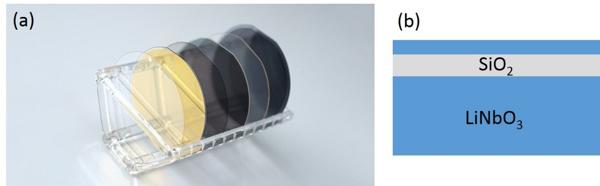
Fig. 1 (a) Monocrystalline LNOI wafer and (b) schematic illustration of the cross section
1 Cutting-edge LNOI fabrication technologies
It begins with an introduction on varies fabrication techniques developed for achieving high quality nanophotonic structures in the ion-sliced monocrystalline thin film, including lithographic argon ion milling, focused ion beam milling, femtosecond laser micromachining combined with focused ion beam milling, electron-beam/ultraviolet lithography followed by argon ion milling, chemo-mechanical polishing, and photolithography assisted chemo-mechanical etching (PLACE) (Fig. 2).
Fabrication technique based on focused ion beam milling provides the highest fabrication resolution, however, the milling area is limited to be less than 1 mm2. Argon ion milling is CMOS compatible, while it will induce lattice damage of LN. PLACE was used to produce large-scale PIC with ultra-smooth surface, however, it is difficult to fabricate structures with wavelength-scale coupled gap. Until now, the propagation losses of the optical waveguides and the Q factors of optical microresonators have been improved to be 3 dB/m and 1.5×10⁸ at 1550 nm wavelength.
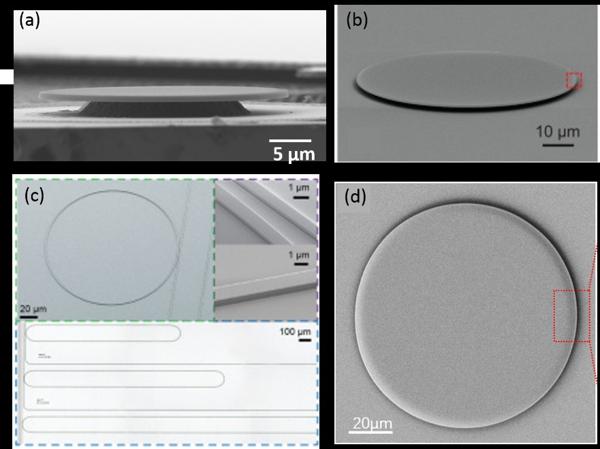
Fig. 2 Optical microresonators fabricated by (a) femtosecond laser micromachining combined with focused ion beam milling, (b) ultraviolet lithography followed by argon ion milling, (c) electron beam lithography followed by argon ion milling and SiO2 coating, (d) PLACE.
2 Domain patterning methods
Different domain polarization methods such as microelectrode poling, piezoelectric force microscopy (PFM)-tip poling, electron beam lithography poling, and ion sliced thin film from periodically poled LN (PPLN) bulk (Fig. 3), have been developed for utilizing the highest nonlinear coefficient d33. Here, only microelectrode poling can be applied on X-cut thin film, thus when the domain patterning is aligned in the Y direction, the largest nonlinear coefficient and electro-optic coefficient can be harnessed simultaneously for PIC.
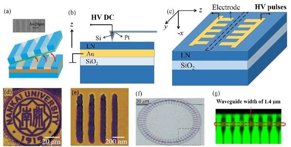
Fig. 3 (a) Schematic diagram of the ion slicing thin film from pre-poled LN. Inset: PPLN thin film. Schematic diagrams of the PPLN thin film fabricated by the (b) atomic force microscope/piezoelectric force microscopy (AFM/PFM) poling method and (c) microelectrode poling method with a high-voltage (HV) direct-current (DC) source. PFM images of (d) logo of Nankai University and (e) PPLN strips with period of 200 nm width and a duty ratio of 50%. (f) SEM image of a PPLN microring with EBL poling. (g) Second-harmonic confocal microscopy of the PPLN thin film fabricated by microelectrode poling.
3 Photonic devices for PICs
Thanks to the rapid development of microfabrication techniques, various types of LNOI devices with unprecedented performances and compact sizes were recently demonstrated (Fig. 4). The development and application of LNOI-based PIC devices have been demonstrated, such as electro-optic modulation with 100 GHz bandwidth and 2.2 V·cm half-wave voltage length product, acoustic optics, nonlinear optics ranging from classical/quantum light sources to frequency combs, and some large-scale PICs.
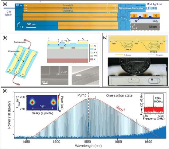
Fig. 4 (a) High speed Mach-Zehnder modulator. (b) High speed Si/LN hybrid modulator. (c) Optical true delay line based on the LNOI. (d) Soliton frequency comb generation.
4 Conclusion and future perspective
The LNOI photonic technology is evolving toward higher performance, higher integration density, and lower production cost. These demands will lead the way for technological development and industrialization of LNOI photonic devices and systems in the future.
However, a series of tasks, such as optimizing of device design and fabrication, developing new fabrication technique for large-scale high-throughput mass production, and integrating LN devices with III–V compound semiconductor devices for on-chip laser sources and detectors, must still be accomplished before the LNOI photonic technology can be widely adopted as a major PIC platform. From the economic point of view, the cost of a LNOI wafer is still high compared to that of an SOI wafer and must be significantly reduced. To be compatible with today's CMOS production line, the size of an optics-grade LNOI wafer should be gradually increased from the current size of 6 inch to 8, 10, and 12 inch to allow for a large-scale fabrication based on deep-ultraviolet lithography.