Conventional photodiode detectors made of crystalline semiconductor materials may have special requirements on fabrication affecting device integration, and their response wavelengths are limited by bandgaps, thereby causing limitation on many applications. Comparatively, plasmonic hot electron photodetectors are advantageous in these aspects. The desired response waveband can be obtained by employing appropriate materials and the response spectrum can be adjusted with designed plasmonic characteristics. Therefore, such a type of photodetectors has a broad application prospect in the field of integrated photonics. However, plasmonic hot electron photodetectors require the fabrication of nanostructures, mostly relying on electron beam lithography at present. Not only the process cost is high, but also large-area fabrication is challenging.
In order to provide a solution to this challenge, a nanocone array template is formed on a silica substrate by plasma etching using a monolayer polystyrene nanosphere mask. Metal-semiconductor-metal films are successively deposited on the template, forming an MSM structure for photodetector devices. This work is carried out by Prof. Ting Mei’s group from the Shaanxi Key Laboratory of Optical Information Technology, Northwestern Polytechnical University. The related results are published in Photonics Research, Vol. 7, No. 3, 2019 (Zhiqiang Yang, et al., Silica nanocone array as a template for fabricating a plasmon induced hot electron photodetector).
The nanostructures enable surface plasmon excitation by the incident electromagnetic waves, and propagation of surface plasmon polaritons along the Au interface enhances optical absorption in the Au film. Hot electrons are generated due to plasmon decay, and those with energy larger than the Schottky barrier are emitted over the barrier into the TiO2 layer and eventually reach the Al electrode, accomplishing photoelectric conversion. Especially under an external bias, the response of the device increases, and its response peak gradually shifts red, indicating that the tunneling effect of hot electrons increases with increasing bias voltage. The researchers also use finite element simulation and related numerical theory to confirm the experimental results. In this work, costly electron beam lithography is avoided and the size of the device reaches centimeter level, which will be advantageous for the integration of hot electron photodetectors with a vast variety of optoelectronic and microelectronic devices.
Prof. Mei believes that this work not only gives a new fabrication process for plasmonic hot electron devices compatible for low-cost large-scale monolithic integration, but also provides theoretical guidance on the excitation and transport processes of hot electrons.
Further work will focus on studying nanostructures with stronger plasmon resonance on the basis of which to increase the optical absorption in metal and the efficiency of hot electron generation, and to improve the quantum efficiency of the device.
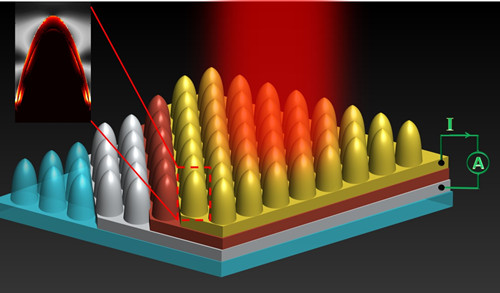
Device architecture of a plasmonic hot electron photodetector based on a silica nanocone template. Hot electrons are excited due to plasmon decay in the Au film and then travel through the TiO2 layer and eventually reach the Al electrode, forming photocurrent.