Inverse design is an attractive and emerging approach to achieve ultra-compact, high-performance, and even new-function integrated silicon photonic devices. Inverse-designed integrated photonic devices can usually have two types of subwavelength structures, "analog" and "digital". For the analog subwavelength photonic device, the cell structure (called "pixel") has a fine size, and the device etched pattern usually has a complex boundary of "arbitrary" bending; its high degree of freedom in inverse design may theoretically achieve high-quality design goals, but the performance of the device is usually greatly affected by fabrication errors. For the digital subwavelength photonic device, the pixel size is generally about an order of magnitude larger, and the device etched pattern has relatively regular rectangular or circular boundaries; the inverse design of digital devices can use simple optimization algorithms to obtain excellent performance and large fabrication tolerance.
The gradient-descent-based adjoint method is indispensable to reduce the ultrafine-pixel-induced tremendous computational cost to a reasonable degree and make the inverse design of analog devices feasible because it could provide the topology or shape gradient information using only a forward and an adjoint (backward) 3D electromagnetic fields simulations regardless of the number of pixels. Unfortunately, the conventional adjoint method can be hardly applied to inverse design of digital devices because one cannot calculate the gradients of a digital pattern. Simple brute-force methods are usually used for optimization of digital patterns. However, the number of 3D simulations in brute-force methods will increase exponentially with the pixel number in a pattern, which may drastically limit the inverse design capability of digital nanophotonic devices.
The research group led by Professor Minming Zhang from Wuhan National Laboratory for Optoelectronics and Huazhong University of Science and Technology proposed and demonstrated a novel digitized adjoint method for high-efficiency inverse design of digital photonic devices.
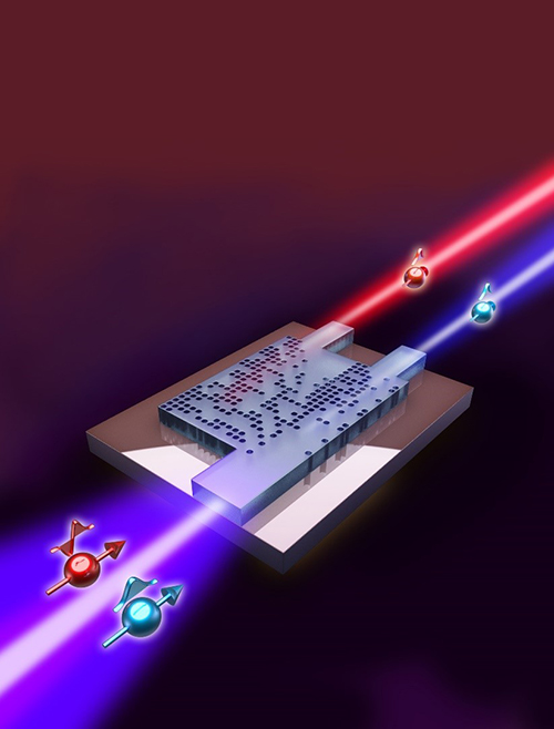
The inverse design process comprises three stages. In the first stage, the adjoint method based on sensitivity analysis is employed to obtain an "analog" pattern with fixed geometric shapes but "grayscale" relative permittivities; in the second stage, a linear-biasing method is used to convert such analog pattern to a "quasi-digital" one in which the relative permittivities of most pixels are close to the two boundary values; in the third stage, the quasi-digital pattern is transformed into an easy-to-fabricated and high-performance N-ary digital pattern based on the equivalent medium theory and fabrication constraints. The researchers designed and experimentally demonstrated a single-mode 3-dB power divider and a dual-mode multiplexer to verify the efficiency and performance of the digitized adjoint method. Related research results are published in Photonics Research, Volume 8, Issue 4, 2020. (Kaiyuan Wang, Xinshu Ren, Weijie Chang, et al. Inverse design of digital nanophotonic devices using the adjoint method[J]. Photonics Research, 2020, 8(4): 04000528)
The digitized adjoint method takes the advantages of adjoint sensitivity analysis and digital subwavelength structure, which could overcome the efficiency bottleneck of the brute-force method that is restricted by the number of pixels of a digital pattern and improve the device performance by extending a conventional binary pattern to a multi-level one. Compared with the typical brute force optimization algorithm, the design efficiency of the digital adjoint method has been improved by nearly 5 times, and approximately the same experimental performances of devices have been achieved.
Professor Minming Zhang believes that this work may create a new way for the efficient and high-performance inverse design of compact digital subwavelength photonic devices, which will help to promote the design automation of inverse-designed integrated photonic devices and their practical applications in on-chip optical interconnection.
Further work will focus on the inverse design of integrated subwavelength photonic devices with complex topologies and novel functions, and exploring their advanced applications in on-chip all-optical signal processing and optical computing.
Digitized adjoint method for high-efficiency inverse design of digital photonic devices