Quantum information science is a new frontier subject combining quantum mechanics and information science. The quantum nature of particle superposition, entanglement, and measurement is applicable for more efficient information processing, computation, transmission, and storage. In the last decades, quantum fundamental science was rapidly transformed into quantum technologies with huge resources invested by global academia, research centers, and industry. Quantum scientific research is moving from the stage of principle verification of quantum rules to the stage of practical device research and development governed by these rules.
Photon, as one ideal information carrier, has been widely used in quantum information processing and shows several unique advantages, such as fast transmission speed, low noise, multiple degrees of freedom for information encoding and high capacity. Besides, light has a wide range of applications in energy, communications, computation, and medical care. These increasingly mature industrial applications provide favorable supports for photonic quantum technologies.
To enhance the complexity of quantum optical experiments, optical quantum systems tend to use integrated photonic circuits. Compared to systems that use discrete optical components on an optical table, the integrated photonic devices enable localization and manipulation of photons at micro/nano scales, thus greatly improving the stability and scalability of quantum optical experiments and providing a complex, compact quantum photonics approach for quantum communications, sensing, and computing applications. Therefore, these integrated techniques will take quantum applications out of the laboratory and into large-scale and practical applications.
Multiple optical materials for quantum integrated photonic device, such as silica, silicon (Si), silicon nitride (SiN), lithium niobate (LN) have been developed. Among those materials, silicon photonics is a good candidate because of its easy preparation, high integration density, and excellent optical properties. Thanks to the leadership of classical silicon photonics in large-scale photonic integrated circuits, the performance of silicon-based devices also has been rapidly improved, and the potential for applications in scalable quantum information processing with silicon is being fully exploited.
The invited review article published in Photonics Research, Vol. 10, No. 10, 2022 (Lantian Feng, Ming Zhang, Jianwei Wang, Xiaoqi Zhou, Xiaogang Qiang, Guangcan Guo, Xifeng Ren. Silicon photonic devices for scalable quantum information applications [J]. Photonics Research, 2022, 10(10): A135-A153) provides a comprehensive overview on the latest research effort and state-of-the-art technologies on silicon photonic chips for scalable quantum applications.
1 Scalable technique for silicon photonic chips
Scalable quantum information processing needs the quantum photonic source, detector, logic operation and other core functions to be improved with high quality and be integrated on the same chip. For photonic source preparation, silicon waveguides have a strong third-order nonlinear response and can be directly used to prepare photon pair sources via a spontaneous four-wave mixing process. After pair generation, one of the photons is detected to herald the presence of its partner. Although each photon pair source is probabilistic, multiple heralded single photons can be dynamically switched to one single output mode, thus increasing the output probability. For example, a 100% enhancement was achieved by multiplexing photons from four temporal modes. On the other hand, the solid-state emitters at telecommunications wavelengths have been demonstrated. In particular, recently demonstrated G centers and T centers, which originate from carbon-related defects in silicon, can be directly integrated into silicon waveguides without hybrid integration for large-scale quantum photonic information applications.
For single-photon-level detection, superconducting nanowire single-photon detectors show excellent performance, such as near-unity system detection efficiency, GHz maximum count rate and picosecond-level temporal resolution. For non-cryogenic applications, other type detectors, such as germanium-on-silicon and InGaAs/InP single-photon detectors, are potential alternatives. In addition to these conventional devices, single-photon detection based on low-dimensional materials is emerging and has shown superior performance.
To adjust photon's frequency and spatial mode degree, integrated wavelength and mode division multiplexing techniques have been demonstrated. Structures like ring resonators, unbalanced MZIs, waveguide Bragg gratings, and arrayed waveguide gratings (AWGs) have been used for wavelength multiplexing and demultiplexing. Mode division multiplexing is an emerging technique that uses the high-order transverse waveguide modes of multimode waveguides to encode more information. Since multimode waveguides still support multiple wavelengths, this technique is compatible with wavelength division multiplexing to further increase the channel capacity. Modulators have achieved high speeds and can even operate at cryogenic temperatures.
Chip interconnection, which will play a key role in building large-scale quantum networks, has been further developed (Fig. 1). For example, grating couplers and end couplers both achieve less than 1 dB coupling loss. In addition to fabricating complex coupling structures on a chip, many other efficient approaches are also worth considering. For example, 3D-printed optical probes on the fiber end faces, photonic wire bonding and in situ 3D nanoprinting.
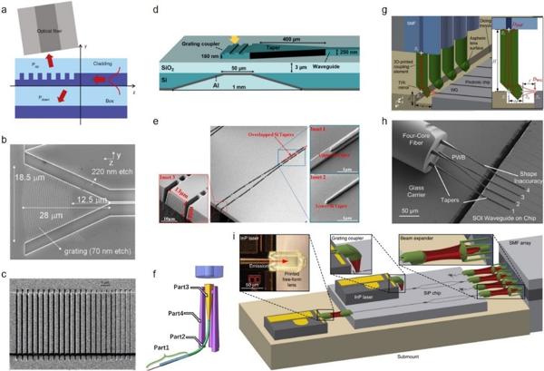
Fig. 1 Chip interconnection techniques in silicon photonics. (a) Diffraction grating-based coupling structure. (b) The focusing grating. (c) The double-etched apodized waveguide grating coupler. (d) The grating coupler with a single aluminum backside mirror. (e) The mode-size converter as end coupler. (f) Coupler structure. (g) The 3D-printed optical probes on the fiber end faces. (h) Fiber cores and different silicon waveguides connected by photonic wire bonds. (i) In situ 3D nanoprinted free-form lenses and expanders.
2 Scalable quantum information applications
The development of integration technology has promoted the progress of quantum applications. In terms of multiphoton and high dimensional applications (Fig. 2), the number of detected photon has achieved 8, the visibility of four-photon interference achieved 96% and 15-dimensional two-photon entanglement demonstrated. Besides, high-dimensional programmable quantum processor has been demonstrated recently. In terms of quantum error correction, the success rate was increased from 62.5% to 95.8% when running a phase-estimation algorithm using the error-correction program. In terms of quantum key distribution, multiple encoding protocols and even high-dimensional chip-to-chip key distribution have been realized. In addition, chip-to-chip quantum state teleportation have been demonstrated by using on-chip multi-photon entanglement.
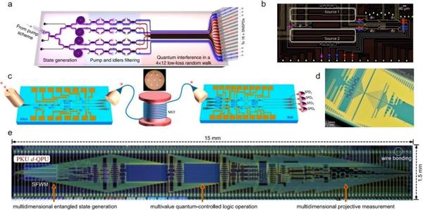
Fig. 2 Multiphoton and high-dimensional applications with silicon photonic devices. (a) Silicon photonic chip for the generation and sampling of quantum states. (b) Coherent pumping of two sources and processing of the emitted photons. (c) Chip-to-chip high-dimensional quantum key distribution based on multicore fiber. (d) Silicon device for multidimensional quantum entanglement. (e) Programmable qudit-based quantum processor.
3 Challenged and outlook
Despite the progress mentioned above, further improvements are needed in some areas for scalable quantum information applications, such as low-loss components, high-quality multiphoton entanglement generation, deterministic quantum operation and frequency conversion. With further upgrading of the fabrication technology, silicon photonics will have greater prospects in quantum information processing. Despite future quantum information processors are most likely to be hybrid with various materials elevated to the extreme, we believe that silicon photonics will play an important role.