Silicon photonics has rapidly emerged as one of the most prominent technological platforms for the implementation of integrated optical devices. Its compatibility with standard complementary metal-oxide-semiconductor transistor (CMOS) fabrication processes, has enabled low-cost and high-volume manufacturing, making silicon photonics suitable for the implementation of high bit-rate transceivers for data-centre and direct-detection scheme applications. At the same time, silicon photonics technology has been in the forefront for the realization of a number of integrated components for various applications ranging from sensors to microfluidics.
Historically, one of the biggest challenges in designing silicon photonic components, has been related to the realization of high-performance mode converters which can efficiently transfer the light from a standard optical fibre to the integrated circuits. Indeed, this task is particularly challenging due to the strong intrinsic birefringence of integrated silicon waveguides, and to the large size mismatch existing between the optical mode of silicon waveguides and that of single mode fibres (which is almost 800 times larger).
To overcome this issue, the scientific community has proposed different solutions over the last 20 years, which can be schematically divided into two main categories: “end-fire” and “vertical” coupling techniques. In “end-fire” configurations the optical coupling takes place at the edge of the chip in a direction parallel to the chip surface thanks to spot size converters; conversely “vertical” coupling occurs when the incoming beam impinges on the silicon chip almost perpendicularly to its surface and takes advantage of diffractive grating couplers to re-direct the incoming radiations.
Both coupling strategies have different strengths and weaknesses, in terms of performance and ease of fabrication, and can in turn be divided into many different sub-categories, according to the specific design approach employed, and to the chosen materials and fabrication technology.
The group led by Dr. Cosimo Lacava from the Optoelectronics Research Centre, University of Southampton, provides a comprehensive scientific description and view of the various possible solutions that researchers have produced over the last years. They provide the reader with an exhaustive analysis of more than 70 structures reported in the literature, characterized by different level of design and fabrication complexity.
In the review they first describe the physical phenomena underlying the optical coupling mechanism; then they analyze the different coupling solutions available, in terms of their performance (such as coupling efficiency, bandwidth, polarization sensitivity and alignment tolerances) and their compatibility with standard CMOS process flows and packaging techniques. For the benefit of the reader, they benchmark the various coupling solutions against each other in a table at the end, providing the reader with a useful reference, without the need to scan the entire review. This work is published in Photonics Research, Volume 7, Issue 2, 2019 (Riccardo Marchetti, et al., Coupling strategies for silicon photonics integrated chips).
Dr. Cosimo Lacava comments on this work: “The ability to couple a light beam from a SM-fibre to a nanophotonic circuit has always represented a significant challenge for researches working in this field. Although the wording of the problem is simple (How we squeeze the light into a waveguide, which is 800 times smaller than an optical fibre without losing too much energy?), the physics involved is intriguing and technologically complex, and has inspired many scientists who have developed a number of elegant solutions over the years. If you are starting your career as silicon photonic engineer or simply you are looking at the various solutions available to couple the light to your designed integrated circuit, here we provide a comprehensive reference, containing the most common techniques and solutions to accomplish this basic task, vital for the realization of any modern integrated component.”
They believe that future work in the field will be focused on the development of even more efficient coupling structures, where the effort to reduce the couplers insertion loss will have to cope with the necessity to attain full CMOS compatibility and reduction of assembly time and cost, in the perspective of mass-markets manufacturing.
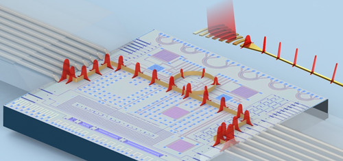
Schematic of a Silicon Photonics circuit. Arrays of angle-polished and planar polished fibres are respectively used to couple the grating- and edge-couplers integrated on the chip. An enlarged schematic of a grating is shown at the top.