3D and flexible devices benefit from many advantages over their rigid counterparts, including amenability to large-area, low-cost fabrication via roll-to-roll processing, and the possibility of conformal integration on curvilinear surfaces or biological tissues. Following in the footsteps of the widely successful 3D electronics, 3D integrated photonics has recently attracted increasing attention in an effort to provide the same deployment flexibility to optical systems, with applications covering biotechnology, sensing, 3D manufacturing, optical interconnects, and others. 3D integrated photonics is thus poised to expand the reach of photonics by enabling both the extension of traditional applications to non-planar geometries and adding novel functionalities that cannot be attained with planar devices.
However, the geometries and materials used in existing 3D integrated photonic systems are limited by the current fabrication methods: demonstrations of 3D integrated photonic devices to date are either topologically 2D (curvilinear) in nature or rely on specialized material systems (photosensitive glasses or polymers, for instance). As an application example, the much-needed ability to monitor stress in biological samples such as cell cultures and tissue models requires a platform that provides precise measurements at multiple, pre-defined locations in 3D, which none of the current fabrication methods for 3D integrated photonics can offer.
The research groups from MIT led by Prof. Juejun Hu and University of Delaware led by Prof. Xinqiao Jia demonstrate, for the first time, 3D integrated photonic devices with arbitrary geometry. Related research results are published on Photonics Research, Vol. 8, Issue 2, 2020 (Jérôme Michon, Sarah Geiger, Lan Li. 3D integrated photonics platform with deterministic geometry control[J]. Photonics Research, 2020, 8(2): 02000194), and were selected as Editors’ Pick.
The novel fabrication process deterministically yields the pre-defined final shape of the device, such that the spatial location of any component within the device is chosen and controlled by the user. The process relies on standard planar fabrication of the photonic device on top of a rigid handler substrate, followed by its delamination from the handler and deterministic deformation into a 3D structure, much like the way pop-up books work.
The final structure consists in several buckled strips joining two planar edge platforms, as shown on Fig. (a). Each strip may contain waveguides and waveguide-coupled components such as resonators. The input/output light coupling ports are located in the edge platforms, where they can interface with non-integrated optics (fibers, lenses) using standard coupling schemes such as grating coupling and edge coupling. To predict and control the final shape of the buckles, the authors rely on large-deformation beam bending theory. A variety of buckle shapes is made possible by considering several segments of varying moment of inertia, thereby providing additional degrees of freedom to the system (in this case, the length and thickness of each segment along the strip). They expand the traditional beam-bending formulae to the case of multi-segment beams, and show that the fabricated devices (see Fig. (b)) precisely match theoretical shapes.
To demonstrate the practical applications of the platform, the authors package the devices with fiber arrays. Fiber array bonding not only represents a scalable and robust coupling scheme, but also eliminates the need for further optical alignment, thus allowing for easy, remote probing of the device. Finally, they demonstrate the ability to use this platform for 3D sensing by calibrating its stress-sensing response. Stress-induced optical effects must first be isolated from other interfering effects (such as this of temperature) in order to achieve high-sensitivity sensing. Reference, temperature-tracking sensors are used to decouple the influence of temperature and stress. Then the authors compare optical measurements and mechanical simulations to link the optical response to applied strains, eventually yielding the device's stress-optical coupling coefficient. Given the high accuracy of wavelength measurements, the results indicate a strain measurement accuracy of 0.01%, for materials with a Young's modulus down to 300 Pa.
The fabrication approach for 3D integrated photonics offers a number of key advantages. First, it leverages standard planar processing technologies used in the fabrication of traditional integrated photonics, thus allowing for high-quality optical components. This also ensures compatibility with most materials commonly used in integrated photonics, which can be either directly deposited and processed on a polymer substrate, or transferred onto the substrate. Second, this approach enables construction of 3D architectures by controlled, deterministic mechanical deformation, as outlined in the previous paragraph. Third, it is readily scalable to a large number of sensing channels. Additional probing points can be created simply by increasing the number of lithographically defined strips and by multiplexing several optical sensors along each waveguide, without compromising the quality and throughput of fabrication. Finally, as this platform is based on standard optical components, it allows for compatibility with common optical coupling and packaging schemes, such that devices can be readily used outside optical laboratories.
Given the wide range of physical and chemical sensing applications of optical resonators, as well as the possibility to multiplex resonators spectrally and spatially, it is also amenable to monitoring a variety of parameters at a large number of locations in a distributed sensor array. This platform thus potentially enables multifunctional sensing, mapping, and light delivery in the 3D space, opening the door to further research in this area.
Prof. Juejun Hu, who directed this research, says: “The world we live in is not flat, so integrated photonics ought not to be flat, either. Being able to access the third and long-missing dimension is useful for applications where 3D information is valuable such as sensors for mapping complex variables and light conduits or receptors for delivering/capturing photons to/from different locations.”
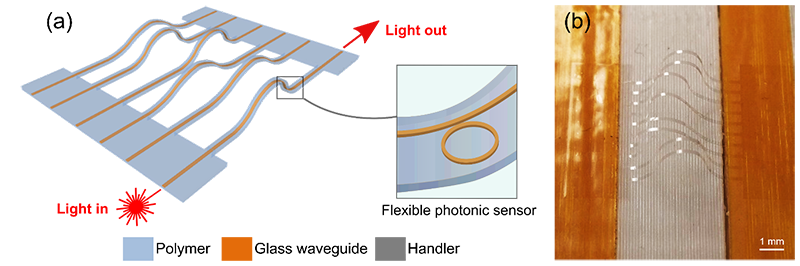
(a) Schematic of the 3D device layout. (b) Picture of a fabricated 3D device.