Analog-to-digital converters (ADCs) along with their counterparts the digital-to-analog converters (DACs) are an indispensable link between our analog physical world and the virtual digital world where data are stored and processed digitally. Besides, the transmission of such data is required to be at high-speed in the current high-capacity communication networks, which are likely to be optical. Driven by advanced applications such as optical communications, imaging and Lidar systems, better performance ADCs and DACs that are also scalable are constantly in demand. The existing ADCs deployed in our current applications are mostly implemented in the electronic domain as integrated circuits where vast amount of circuitry is needed to perform the complex operations that are necessary to quantize the continuous signal into a stream of high-fidelity discrete data. The amount of processing effort of these components often limits the performance of the electronic ADCs and the users are left with the choice of speed versus fidelity. In photonics applications, methods that can digitize the analog optical signal without the need for optical-electrical conversion are preferred because the operation can be done passively and they can improve the operation speed while lowering the power consumption at the same time. There has been an extended effort in the development of such photonic ADC solutions and many have been proposed and demonstrated in recent years. In general, nonlinear optical fiber and bulk optics-based systems have better performance metrics but they are bulky and are not scalable. Integrated photonic ADCs, which are scalable and mass manufacturable have become the research focus of current most advanced high-performance photonic ADCs field.
Here, the authors propose and demonstrate a photonic ADC that utilizes the Kerr nonlinearity in a specially designed optical waveguide as the key element for the all-optical digital-to-analog conversion. Relevant research results are published in Photonics Research, Volume 7, Issue 10, 2019, and selected as Editors’ Pick by Editor-in-Chief. ( Yuhua Li, Kun Zhu, Zhe Kang, Wai Lok Ho, Roy Davidson, Chao Lu, Brent E. Little, Sai Tak Chu. CMOS-compatible high-index doped silica waveguide with an embedded silicon-nanocrystal strip for all-optical analog-to-digital conversion[J]. Photonics Research, 2019, 7(10): 1200-1208 )
The specially designed integrated optical waveguide simultaneously possesses high nonlinearity and low transmission loss, and can directly quantize the optical sampling signal almost instantaneously at femtosecond response time and at low power consumption levels. When an optical pulse passes through the highly nonlinear optical waveguide in the proposed photonic ADC, it results in a specific degree of spectral broadening and splitting as a function of its optical power due to the self-phase modulation effect. Utilizing this effect, one can relate the power variation of the pulses to the frequency variation, in other words, the power level is being sorted into the different frequencies and all one has to do is to check the frequency components of the output signal to determine the power of the pulse. Hence, high-speed all-optical digital-to-analog conversion can be achieved by filtering, detecting, binary decision and encoding the spectrum output from the waveguide at the specific wavelengths. In the demonstrated ADC, the optical waveguide used in the experiments is a 50 cm long high-index doped silica glass waveguide with an embedded strip of approximately 20nm thick silicon-nanocrystal (Si-nc). The full length of the waveguide can fit into a 2 mm x 2 mm area, making it highly scalable. We have shown that the addition of the highly nonlinear Si-nc layer provides a three-fold increases in the nonlinearity of the waveguide or approximately 20 and 100 times larger than that of the highly nonlinear fibers and dispersion-shifted fibers, respectively. Besides the enhanced nonlinearity, the addition of the Si-nc layer only increases the propagation loss to the manageable level of 0.16 dB/cm in the telecom band. As a proof of concept, the authors used a commercial C-band femtosecond laser and the filtering and monitoring at two specific wavelengths and demonstrated a low power consumption 2-bit photonic ADC with energy efficiency of 19.55 pJ/bit. One can expect the number of bits of the ADC can be increased with a longer waveguide and with better fiber to waveguide coupling, with the increased number of bits, the per bit energy efficiency will be improved accordingly. Compared with other photonic ADCs such as the fiber-based devices, the proposed ADC here is more compact and with lower power consumption. More importantly, the fabrication process of the optical waveguide is fully compatible with CMOS processes where the filtering elements for frequency sorting can be fabricated on the same chip, thus has the added potential for low-cost on-chip mass production.
Dr. Sai Tak Chu, who leads this research effort, mentions that owing to the nonlinear optics effect, it is now possible to sort the power level of the input signal passively and reduces the complexity of the circuitry. The simplicity of the design has the added benefits of higher speed and lower power consumption. With this encouraging result, he states that the on-going task is to improve the performance and to expand the scope of the proposed ADC device by further optimize the nonlinearity, dispersion, propagation and insertion losses of the optical waveguide toward the realization of a fully integrated photonic ADC where all the necessary components are integrated onto the same chip.
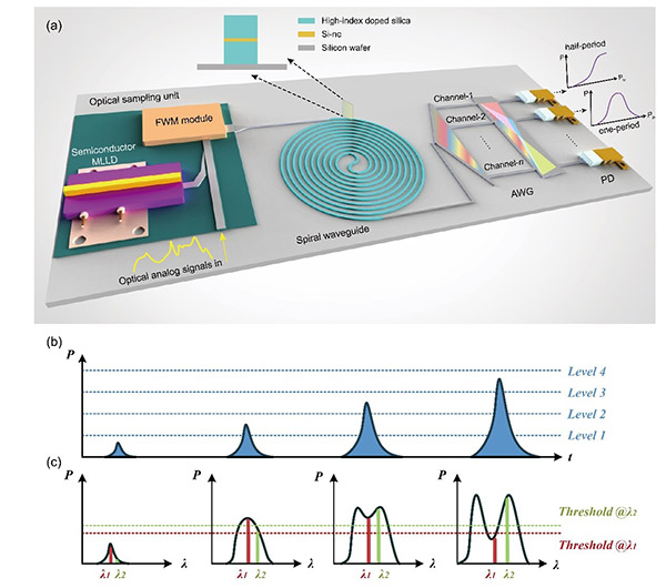

(a) Schematic diagram of the proposed all-optical ADC. (b) Illustrated four sampled pulses with different optical power levels. (c) Corresponding optical spectrum broadening and splitting. Solid lines indicate the decision channel while dashed lines indicate the decision thresholds.