In recent years, the 2 μm waveband has attracted increasing research for broad applications, including optical communication, optical sensing, and even the next generation of gravitational-wave observatories. Particularly, thanks to hollow-core fibers with low latency and low loss in an ultrawide bandwidth, and thulium (Tm) doped fiber amplifiers with a broad gain spectrum, 2 μm possesses the promising application of next-generation optical communication with ultralow latency and further higher capacity. Several 2 μm optical short-reach interconnections over hollow-core fibers have been carried out in our previous works, achieving a record single-lane speed of 100 Gbps. Meanwhile, the photonic integrated platform for 2 μm optical interconnection is also an essential field that needs to be exploited.
Till now, fabrications of mid-infrared (MIR) waveguides have been demonstrated in different platforms, including silicon-on-insulator (SOI), germanium-on-silicon, silicon-on-sapphire, silicon nitride, indium phosphide, and chalcogenide glasses (ChGs). In the range near 2 μm, the majority of integrated waveguides are still fabricated on SOI. However, chalcogenide (ChG) materials, with broadband infrared transparency (0.8~20 μm) and lower two-photon absorption α2 (0.01~1×10-12 m/W) than silicon, have extremely low linear and nonlinear propagation loss at 2 μm. With a relatively high refractive index of n ≈ 2-3, more compact on-chip integration can be realized on ChG. Thanks to the slower slop of refractive index v. s. wavelength and waveguide width, ChG components natively present a wider optical bandwidth and less sensitivity to the fabrication deviations. In a word, all of the merits mentioned above make the low loss at 2 μm and high-density integration of ChG optical devices possible.
Besides, a high nonlinear coefficient makes ChG realizable to obtain efficient nonlinear effect at lower pump threshold, like stimulated Brillouin scattering. As a result, ChG have been widely studied for on-chip all-optical signal processing, including frequency comb generation, supercontinuum generation, wavelength conversion and so on. In addition, since it's easy to deposit ChG films on many substrates like conventional silicon or polymer substrates at low temperature (<300℃), ChG can be part of hybrid waveguides for 2 μ- photonic integrated chips with other materials. Overall, holding various characteristics covering wide application range, ChGs present a significant and promising integrated platform, particularly for 2 μm optical communications.
ChG photonic integrated circuit for improved 2 μm optical interconnection was presented in Photonics Research, Volume 8, Issue 9, 2020 ( Weihong Shen, Pingyang Zeng, et al. Chalcogenide glass photonic integration for improved 2 μm optical interconnection[J]. Photonics Research, 2020, 8(9): 09001484.), under the cooperation between the research group of Prof. Jiangbin Du, Prof. Zuyuan He from Shanghai Jiao Tong University and that of Prof. Bin Zhang, Prof. Zhaohui Li from Sun Yat-sen University.
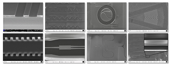
The researchers build up the ChG integrated platform with 600-nm-thick As2S3 strip waveguide on silicon dioxide substrate, and design several key passive components for 2 μm optical interconnection. The fabricated strip waveguide with single mode at 2 μm has low propagation loss of 1.4 dB/cm. The fiber-to-chip vertical coupling loss is optimized at 4.3 dB/facet with 123.6 nm 3 dB bandwidth around 2 μm, which is nearly 2 times wider than the grating bandwidth on SOI, so that further broadband wavelength division multiplexing (WDM) at 2 μm can be realized on ChG platform. Other essential components including Bragg grating filter, power splitter, Mach-Zander interferometer (MZI), and mode converters for on-chip mode division multiplexing (MDM), are also designed and fabricated at 2 μm with highly reliable performances. Mode converters for 2 higher-order modes present the insertion loss of less than 2 dB, crosstalk of less than -20 dB in a wide range, and the fabrication tolerance of waveguide width shows improved - 1 dB bandwidth of 40 nm. Finally, by means of the proposed As2S3 platform, they report a demonstration of on-chip MDM transmission at 2 μm, achieving total bit rate of 3×80 Gbps with error-free bit error rate lower than 3.8×10⁻³, which holds 12 times larger capacity than that of the previous results, and breaks the record of total capacity for 2 μm optical communication.
Prof. Jiangbing Du from Shanghai Jiao Tong University believes that, ChG platform draws the promising prospect for the future photonic integration and high-speed interconnection at 2 μm waveband. The low propagation loss and reliable devices with broadband operation and large fabrication tolerance make the ChG platform capable of holding broadband WDM and MDM simultaneously, so as to achieve ultrahigh-speed interconnection at 2 μm. Furthermore, other essential components such as arrayed waveguide grating for 2 μm WDM can be designed on the proposed ChG platform in the future, in order to further increase the total capacity of 2 μm optical interconnection.
ChG photonic integrated key components for 2 μm optical interconnection